

Electronic component, and a method of manufacturing an electronic component
a manufacturing method and electronic technology, applied in the field of electronic components, can solve the problems of programming conventional memory cells that may require high power consumption, local temperature increase, flash memory scaling beyond 45 nm nodes becoming a real problem,
Inactive Publication Date: 2015-09-22
TAIWAN SEMICON MFG CO LTD
View PDF27 Cites 0 Cited by
- Summary
- Abstract
- Description
- Claims
- Application Information
AI Technical Summary
Benefits of technology
This configuration enables phase change memory cells with reduced power consumption, low threshold voltage, and small lateral dimensions, facilitating downscaling and efficient programming with moderate power demands.
Problems solved by technology
In the field of non-volatile memories, flash memory scaling beyond a 45 nm node has become a real issue.
A high current density caused by the pulse may lead to a local temperature increase.
Method used
View moreImage
Smart ImageViewing Examples

Examples
embodiment 1800
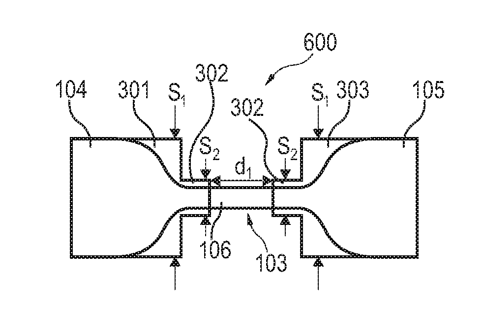
[0088]FIG. 15 shows an embodiment 1800 in which only a small portion of the narrow portion 107 overlaps with the respective electrodes 101 or 102.
[0089]FIG. 16 shows a conventional structure 1900 in which no overlap occurs, resulting in a large amorphous spot, therefore yielding a high threshold voltage.
embodiment 2000
[0090]FIG. 17 shows another conventional embodiment 2000 in which a bar-bell shaped phase change line 103 is applied on two rectangular electrodes 101, 102 to form the non-overlapping structure 2000.
Login to View More PUM
 Abstract
An electronic component (100), a first electrode (101), a second electrode (102), and a convertible structure (103) electrically coupled between the first electrode (101) and the second electrode (102), being convertible between at least two states by heating and having different electrical properties in different ones of the at least two states, wherein the convertible structure (103) comprises terminal portions (104, 105) connected to the first electrode (101) and to the second electrode (102), respectively, and comprises a line portion (106) between the terminal portions (104, 105), the line portion (106) having a smaller width or thickness than the terminal portions (104, 105), and wherein the convertible structure (103) is arranged with respect to the first electrode (101) and the second electrode (102) so that, in one of the at least two states, the line portion (106) has an amorphous ‘Spot (107) extending along only a part of the line portion (106).
Description
CROSS REFERENCE TO RELATED APPLICATIONPriority[0001]This application is a United States national phase application of co-pending international patent application number PCT / IB2008 / 052391, filed Jun. 18, 2008, which claims priority to European international patent application No. 07110692.6, filed Jun. 20, 2007, the disclosures of which are incorporated herein by referenceFIELD OF THE INVENTION[0002]The invention relates to an electronic component.[0003]Moreover, the invention relates to a method of manufacturing an electronic component.BACKGROUND OF THE INVENTION[0004]In the field of non-volatile memories, flash memory scaling beyond a 45 nm node has become a real issue. Technologies to face this challenge are ferroelectric, magnetic and phase change memories, the latter one being promising for the replacement of flash and showing characteristic that may allow replacement of other types of memories such as DRAM. Phase change memories are a possible solution for the unified memory be...
Claims
Login to View More Application Information
Patent Timeline
 Patent Type & AuthorityPatents(United States)
IPC IPC(8): H01L47/00H01L45/00H10N80/00
CPCH01L45/06H01L45/1226H01L45/143H01L45/144H10N70/231H10N70/823H10N70/8825H10N70/8828H10N70/20H10N70/882H10N70/063
InventorHURKX, GODEFRIDUS ADRIANUS MARIA
OwnerTAIWAN SEMICON MFG CO LTD