Electronic device comprising a convertible structure

a technology of electronic devices and convertible structures, applied in the field of electronic devices, can solve the problems of high power consumption, local temperature increase, flash memory scaling beyond 45 nm nodes,

Active Publication Date: 2013-02-05
UNITED MICROELECTRONICS CORP
View PDF8 Cites 0 Cited by
  • Summary
  • Abstract
  • Description
  • Claims
  • Application Information

AI Technical Summary

Benefits of technology

[0010]It is an object of the invention to provide an electronic component having a convertible structure that can be programmed with reasonable power consumption.

Problems solved by technology

In the field of non-volatile memories, flash memory scaling beyond a 45 nm node has become a real issue.
A high current density caused by the pulse may lead to a local temperature increase.
However, programming the memory cell according to U.S. Pat. No. 6,800,563 may require high power consumption.

Method used


Image

  • Electronic device comprising a convertible structure
  • Electronic device comprising a convertible structure
  • Electronic device comprising a convertible structure

Examples


Embodiment Construction

[0057]The illustration in the drawing is schematical. In different drawings, similar or identical elements are provided with the same reference signs.

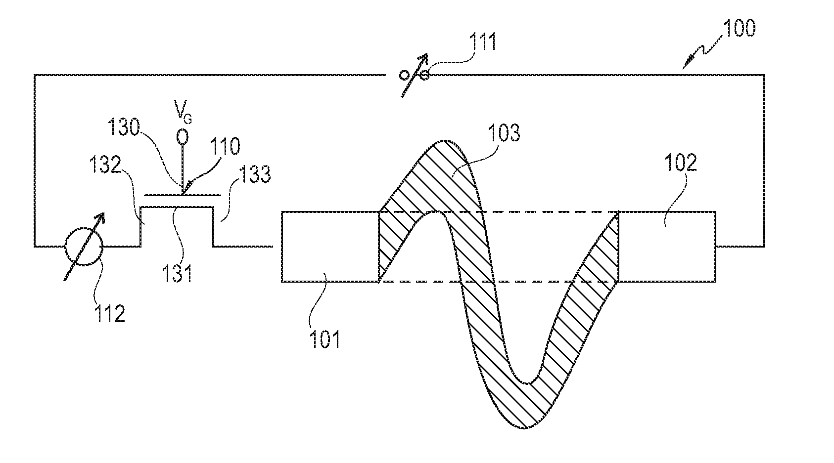
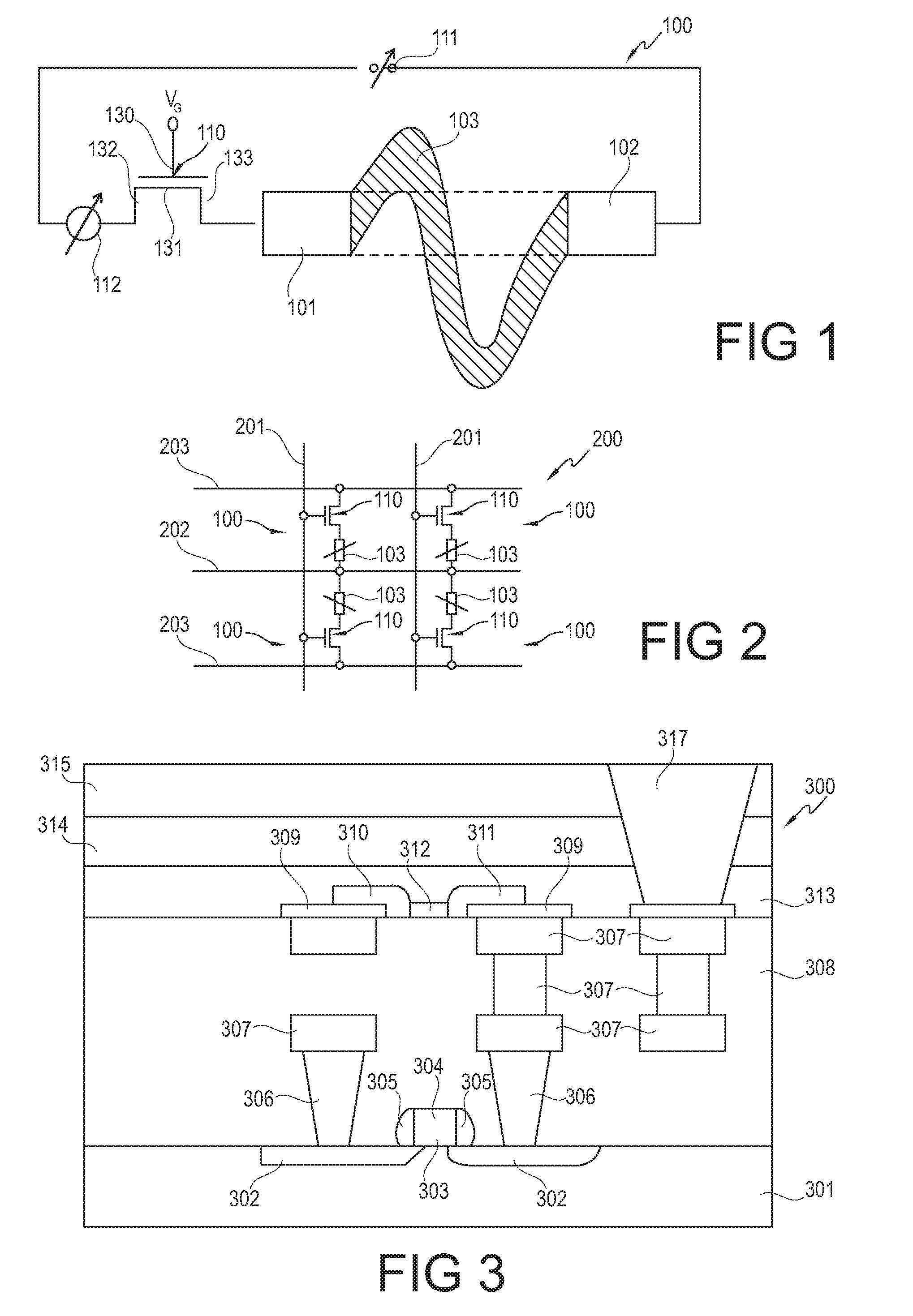
[0058]In the following, referring to FIG. 1, a phase change material memory cell 100 according to an exemplary embodiment of the invention will be explained.

[0059]The memory cell 100 comprises a first electrode 101 and comprises a second electrode 102. Between the first electrode 101 and the second electrode 102, and electrically coupled thereto, a sinusoidal bended phase change material structure 103 is provided which can be converted between a crystalline state and an amorphous state by Joule heating by applying an appropriately high current between the electrodes 101 and 102. In the crystalline state and in the amorphous state, the phase change material structure 103 has different values of conductivity.

[0060]As can be taken from the schematic drawing in FIG. 1, the phase change material structure 103 is curved in a sinusoidal manne...


PUM


Abstract

An electronic device (100), comprises a first electrode (101), a second electrode (102) and a convertible structure (103) connected between the first electrode (101) and the second electrode (102), which convertible structure (103) is convertible between at least two states by heating, wherein the convertible structure (103) has different electrical properties in different ones of the at least two states, wherein the convertible structure (103) is curved in a manner to increase a length of a path of an electric current propagating through the convertible structure (103) between the first electrode (101) and the second electrode (102).

Description

FIELD OF THE INVENTION[0001]The invention relates to an electronic device.[0002]Moreover, the invention relates to a method of manufacturing an electronic device.BACKGROUND OF THE INVENTION[0003]In the field of non-volatile memories, flash memory scaling beyond a 45 nm node has become a real issue. Technologies to face this challenge are ferroelectric, magnetic and phase change memories, the latter one being promising for the replacement of flash and showing characteristic that may allow replacement of other types of memories such as DRAM. Phase change memories are a possible solution for the unified memory being an important step in the electronics art. OTP (“on time programmable”) and MTP (“multiple times programmable”) memories open a field that may present a great opportunity for phase change memories as well.[0004]Phase change memories are based on a reversible memory switching using, for instance, chalcogenide materials. The ability of these materials to undergo fast phase tra...

Claims


Application Information

Patent Timeline
Patent Type & Authority Patents(United States)
IPC IPC(8): H01L29/02
CPCG11C13/0004G11C23/00H01L45/06H01L27/2436H01L45/143H01L45/144H01L45/1675H01L45/1226H10B63/30H10N70/231H10N70/823H10N70/8825H10N70/8828H10N70/063
Inventor TIO CASTRO, DAVIDDELHOUGNE, ROMAIN
Owner UNITED MICROELECTRONICS CORP
Why Eureka
Try Eureka