Semiconductor device

a semiconductor device and semiconductor technology, applied in the direction of discharge tube luminescnet screens, identification means, instruments, etc., can solve the problems of enlargement of display regions entail a reduction in portability, display browsability and portability are difficult to improve, and achieve high portability, high reliability of semiconductor devices, and improved display browsability

Active Publication Date: 2016-01-05
SEMICON ENERGY LAB CO LTD
View PDF39 Cites 31 Cited by
  • Summary
  • Abstract
  • Description
  • Claims
  • Application Information

AI Technical Summary

Benefits of technology

[0008]An object of one embodiment of the present invention is to provide a highly portable semiconductor device and the like. Another object of one embodiment of the present invention is to provide a semiconductor device and the like which provide improved browsability of display. Another object is to provide a highly reliable semiconductor device and the like. Another object is to provide a highly portable semiconductor device and the like which provide improved browsability of display. Another object is to provide a novel semiconductor device and the like.
[0015]According to one embodiment of the present invention, a highly portable semiconductor device and the like can be provided. According to one embodiment of the present invention, a semiconductor device and the like which provide improved browsability of display can be provided. According to one embodiment of the present invention, a highly reliable semiconductor device and the like can be provided. According to one embodiment of the present invention, a highly portable semiconductor device and the like which provides improved browsability of display can be provided. According to one embodiment of the present invention, a novel semiconductor device and the like can be provided.

Problems solved by technology

However, in applications of mobile devices and the like, an enlargement of display regions entails a reduction in portability.
Thus, browsability of display and portability are difficult to improve at the same time.

Method used


Image

  • Semiconductor device
  • Semiconductor device
  • Semiconductor device

Examples


embodiment 1

(Embodiment 1)

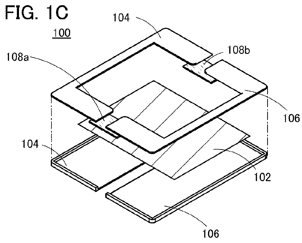
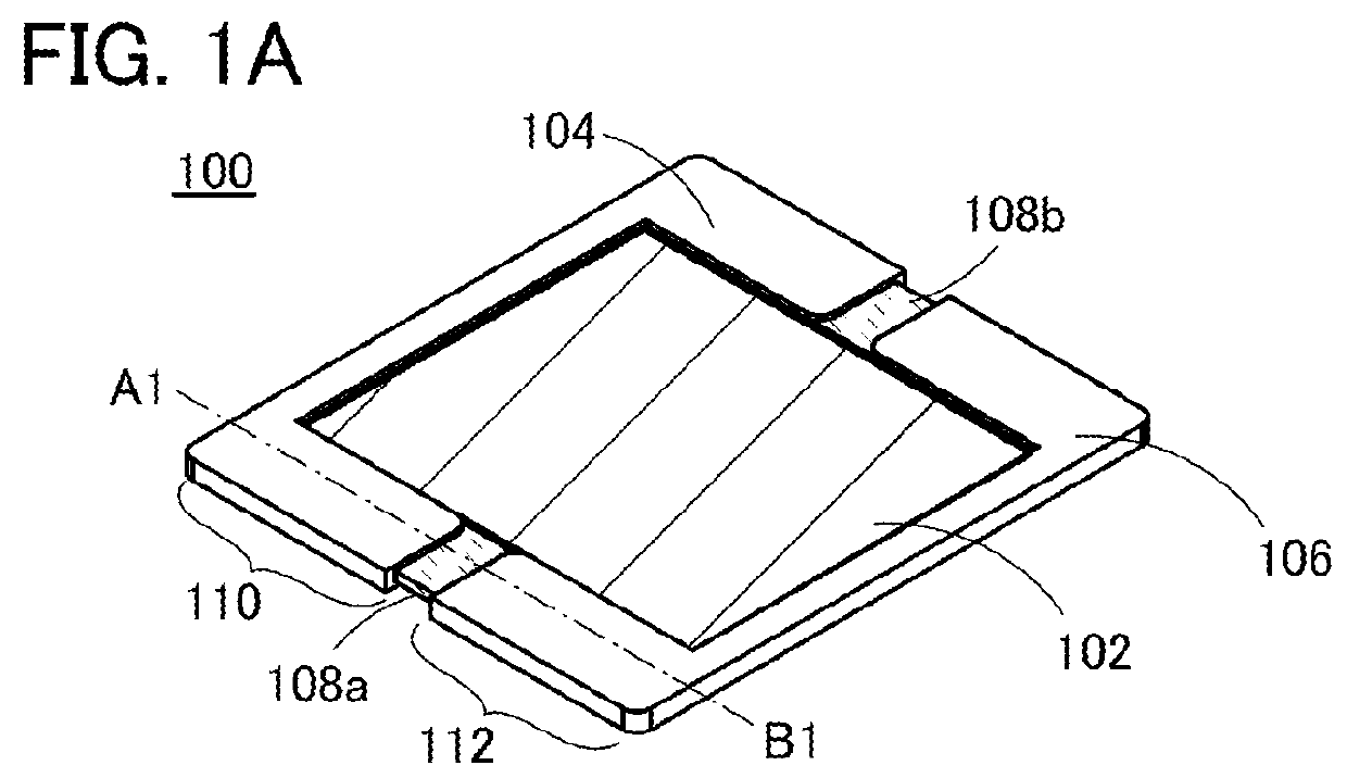
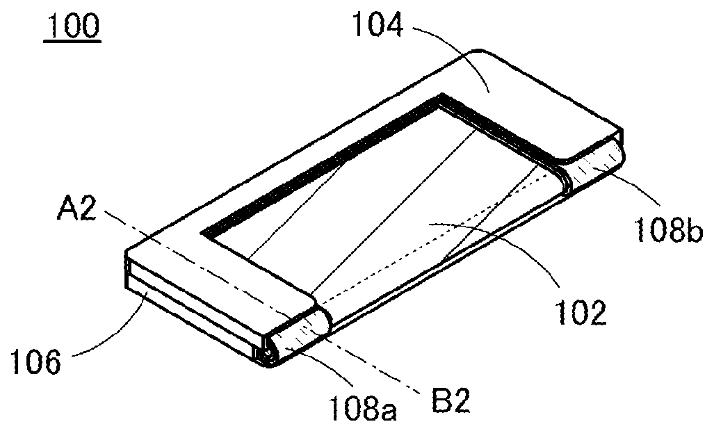
[0039]In this embodiment, a semiconductor device of one embodiment of the present invention is described with reference to FIGS. 1A to 1C, FIGS. 2A to 2C, FIGS. 3A and 3B, FIGS. 4A to 4C2, and FIG. 5. The semiconductor device of one embodiment of the present invention includes a flexible display panel supported by a plurality of housings. The display panel can be deformed into an open position in which regions supported by different housings are substantially on the same plane or into a folded position in which the regions supported by the different housings overlap with each other. A description is made below of an example of a semiconductor device that includes a flexible display panel supported by two housings and can be deformed into a position where the semiconductor device is opened (open position) or into a position where the semiconductor device is folded in two (folded position) by bending the display panel between the two housings.

[0040]FIGS. 1A to 1C illustr...

embodiment 2

(Embodiment 2)

[0090]In this embodiment, an active matrix display panel using an EL element is described as an example of a flexible display panel that can be applied to a semiconductor device of one embodiment of the present invention, with reference to FIGS. 7A and 7B, FIGS. 8A and 8B, FIGS. 9A and 9B, FIGS. 10A and 10B, FIGS. 11A to 11C, and FIGS. 12A to 12C. Note that the display panel is not limited to a display panel including an EL element, and a display panel including a display element such as a liquid crystal element or an electrophoretic element may also be used.

specific example 1

[0091]FIG. 7A shows a plan view of a flexible display panel, and FIG. 7B shows an example of a cross-sectional view of FIG. 7A along the dash-dot line A4-B4.

[0092]The display panel shown in FIG. 7B includes an element layer 1101, a bonding layer 1105, and a substrate 1103. The element layer 1101 includes a substrate 1201, a bonding layer 1203, an insulating layer 1205, a plurality of transistors 1240, a conductive layer 1157, an insulating layer 1207, an insulating layer 1209, a plurality of light-emitting elements 1230, an insulating layer 1211, a sealing layer 1213, an insulating layer 1261, a coloring layer 1259, a light-blocking layer 1257, and an insulating layer 1255.

[0093]The conductive layer 1157 is electrically connected to an FPC 1108 via a connector 1215.

[0094]The light-emitting element 1230 includes a lower electrode 1231, an EL layer 1233, and an upper electrode 1235. The EL layer contains an organic light-emitting material. The lower electrode 1231 is electrically conn...


PUM


Abstract

A highly portable semiconductor device and the like providing improved browsability of display. Provided is a semiconductor device including a flexible display panel, a first housing supporting a first region of the display panel, a second housing supporting a second region of the display panel, and a flexible base material firmly attached to the first housing. The display panel can be deformed into an open position where the first and second regions are substantially on the same plane or into a folded position where the first and second regions overlap with each other. The second housing includes a groove portion where the flexible base material can partly slide. Part of the flexible base material is inserted into the groove portion in the open position. The part of the flexible base material which is inserted into the groove portion is at least partly withdrawn in a deformation into the folded position.

Description

BACKGROUND OF THE INVENTION[0001]1. Field of the Invention[0002]The present invention relates to an object, a method, or a manufacturing apparatus. In addition, the present invention relates to a process, a machine, manufacture, or a composition of matter. In particular, one embodiment of the present invention relates to a semiconductor device, a display device, a light-emitting device, a lighting device, driving methods thereof, or manufacturing methods thereof. In particular, one embodiment of the present invention relates to an electronic device, an information processor, and a communication information device, each of which has a display device, or manufacturing methods thereof.[0003]2. Description of the Related Art[0004]Portable information processors such as smartphones, tablets, and phablets are under active development. For example, an electronic device using a flexible display panel has been known (Patent Document 1). In addition, a multi-panel electronic device has been k...

Claims


Application Information

Patent Timeline
Patent Type & Authority Patents(United States)
IPC IPC(8): H01J1/62G06F1/16H01L27/32H01L51/00
CPCG06F1/1652G06F1/1601H01L27/323H01L51/0097H01L2251/5338G06F1/1677G06F1/3265G09F9/301H04M1/0268Y02E10/549Y02D10/00H10K59/40H10K59/12H10K77/111H10K50/841H10K2102/311
Inventor JINBO, YASUHIRO
Owner SEMICON ENERGY LAB CO LTD
Why Eureka
Try Eureka