Light emitting diode package

a technology of led packages and led components, applied in the direction of semiconductor/solid-state device manufacturing, electrical apparatus, semiconductor devices, etc., can solve the problems of easy collapse or inclined mounting of thin led packages, and achieve the effect of easy collapse or inclined, thin led package, and easy collapse or inclined

Inactive Publication Date: 2016-03-15
SEOUL SEMICONDUCTOR
View PDF22 Cites 1 Cited by
  • Summary
  • Abstract
  • Description
  • Claims
  • Application Information

AI Technical Summary

Benefits of technology

[0044]According to the present invention, a thin LED package is prevented from being easily collapsed or inclined when mounted.
[0045]According to the present invention, a thin LED package includes a support member for preventing the LED package from being easily collapsed or inclined when mounted.
[0046]According to the present invention, a thin LED package is stably installed in a carrier tape pocket when moved or handled during processes.
[0047]According to the present invention, a thin LED package is prevented from being misaligned when moved or handled during processes.
[0048]According to the present invention, a backlight unit includes the LED package.
[0049]According to the present invention, a backlight unit includes the LED package whose height is compensated such that an LED chip is located on the central axis of a light guide plate.

Problems solved by technology

However, the thin LED packages may be easily collapsed or inclined when mounted.

Method used


Image

  • Light emitting diode package
  • Light emitting diode package
  • Light emitting diode package

Examples


Embodiment Construction

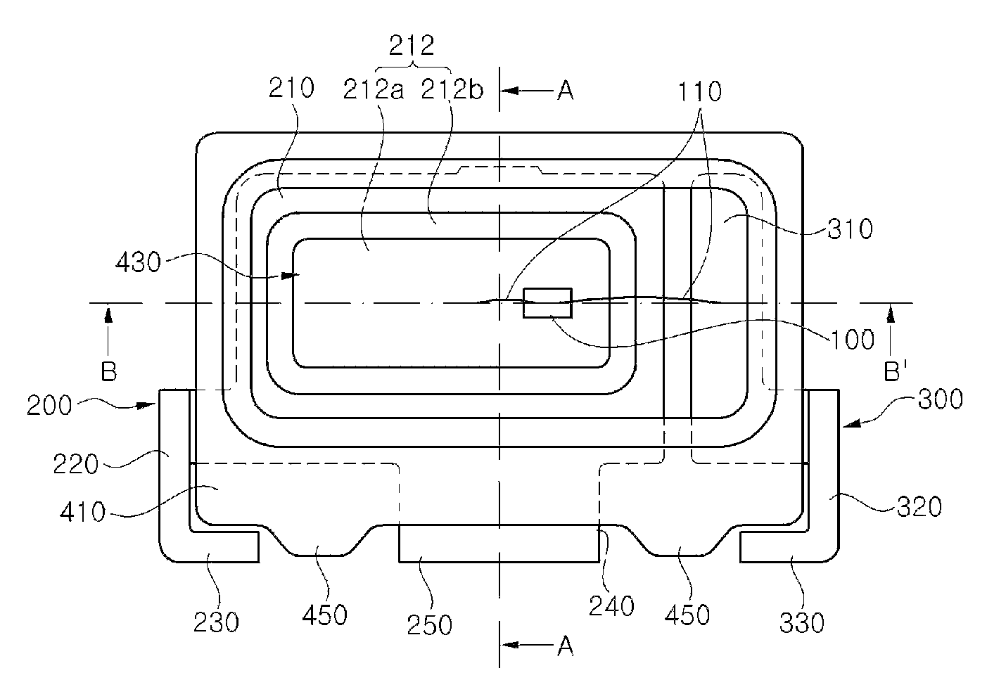
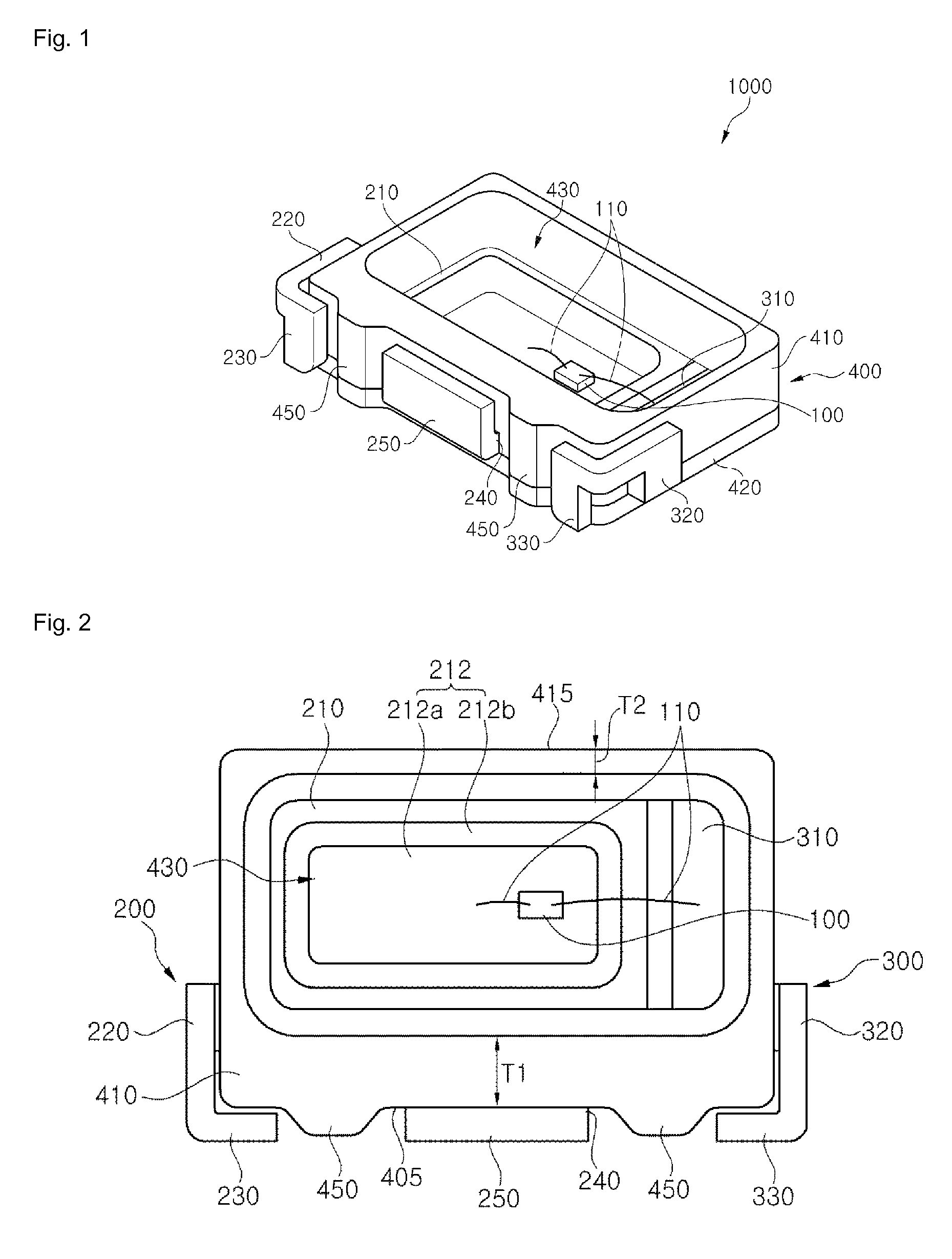
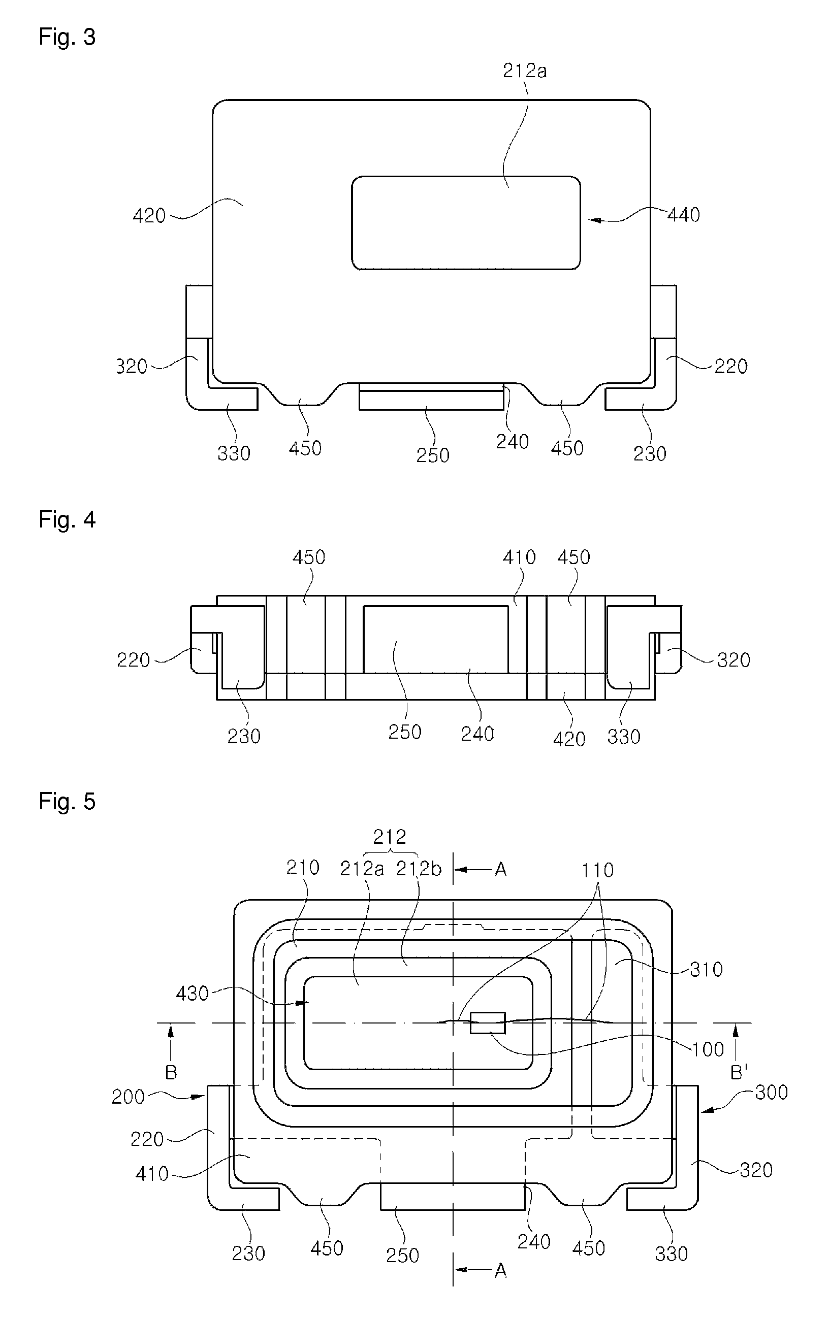
[0083]Exemplary embodiments of the present invention will be described below in more detail with reference to the accompanying drawings. The present invention may, however, be embodied in different forms and should not be construed as limited to the embodiments set forth herein. Rather, these embodiments are provided so that this disclosure will be thorough and complete, and will fully convey the scope of the present invention to those skilled in the art. Throughout the disclosure, like reference numerals refer to like elements.

[0084]FIGS. 1 to 8 are views showing an LED package according to an exemplary embodiment of the present invention.

[0085]FIG. 1 is a perspective view of an LED package according to an exemplary embodiment of the present invention. FIG. 2 is a front view of the LED package shown in FIG. 1. FIG. 3 is a rear view of the LED package shown in FIG. 1. FIG. 4 is a bottom view of the LED package shown in FIG. 1. FIG. 5 is a front projection view of the LED package sho...


PUM


Abstract

An LED package includes a lead frame, a housing part, and a lead heat dissipating part. The lead frame includes a first lead mounting an LED chip and a second lead spaced apart from the first lead. The housing part covers a portion of the lead frame and includes an opening part for exposing the LED chip, a first side corresponding to a support side contacting the first lead and the second lead, and a second side opposite to the first side. The lead heat dissipating part is extended from the first lead and exposed partially to the first side of the housing part. Herein, the first side of the housing part is thicker than the second side.

Description

CROSS-REFERENCE TO RELATED APPLICATIONS[0001]This application is the National Stage entry of International Application PCT / KR2012 / 000800, filed on Feb. 2, 2012, and claims priority from and the benefit of Korean Patent Application No. 10-2011-0055333, filed on Jun. 8, 2011 and Korean Patent Application No. 10-2011-0078257, filed on Aug. 5, 2011, which are incorporated herein by reference for all purposes as if fully set forth herein.BACKGROUND OF THE INVENTION[0002]1. Field[0003]The present invention relates to light emitting diode (LED) packages.[0004]2. Discussion of the Background[0005]A light emitting diode (LED) is basically a PN junction diode that is the junction of a P-type semiconductor and an N-type semiconductor.[0006]An LED has a PN junction of a P-type semiconductor and an N-type semiconductor. When a forward-bias voltage is applied to the P-type semiconductor and the N-type semiconductor, holes of the P-type semiconductor move toward the N-type semiconductor, while ele...

Claims


Application Information

Patent Timeline
Patent Type & Authority Patents(United States)
IPC IPC(8): H01L27/32H01L33/62H01L51/50H01L33/64
CPCH01L33/62H01L27/32H01L33/642H01L33/647H01L51/50H01L2224/48091H01L2224/48247H01L2924/00014H10K59/00H10K50/00
Inventor LEE, JAE JINCHOI, SUNG HOKANG, DUK IN
Owner SEOUL SEMICONDUCTOR
Why Eureka
Try Eureka