

Laser processing apparatus
a laser processing and laser beam technology, applied in metal working apparatus, manufacturing tools, welding/soldering/cutting articles, etc., can solve the problems of difficult to maintain the condition, difficult to set the laser beam focal point on the end surface of the core having a diameter of about 6 m, and difficult to set the laser beam focal poin
- Summary
- Abstract
- Description
- Claims
- Application Information
AI Technical Summary
Benefits of technology
Problems solved by technology
Method used
Image

Examples
Embodiment Construction
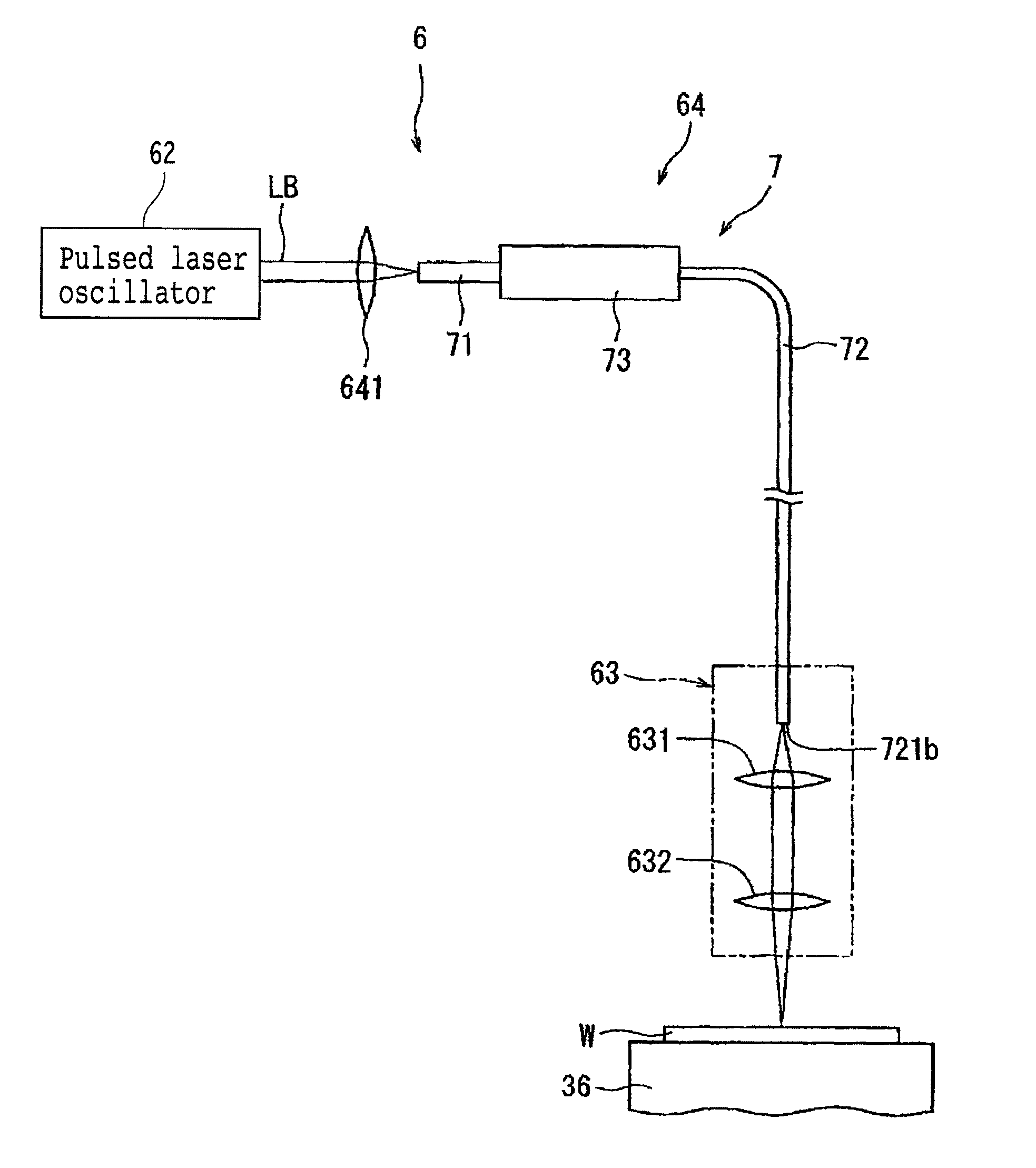
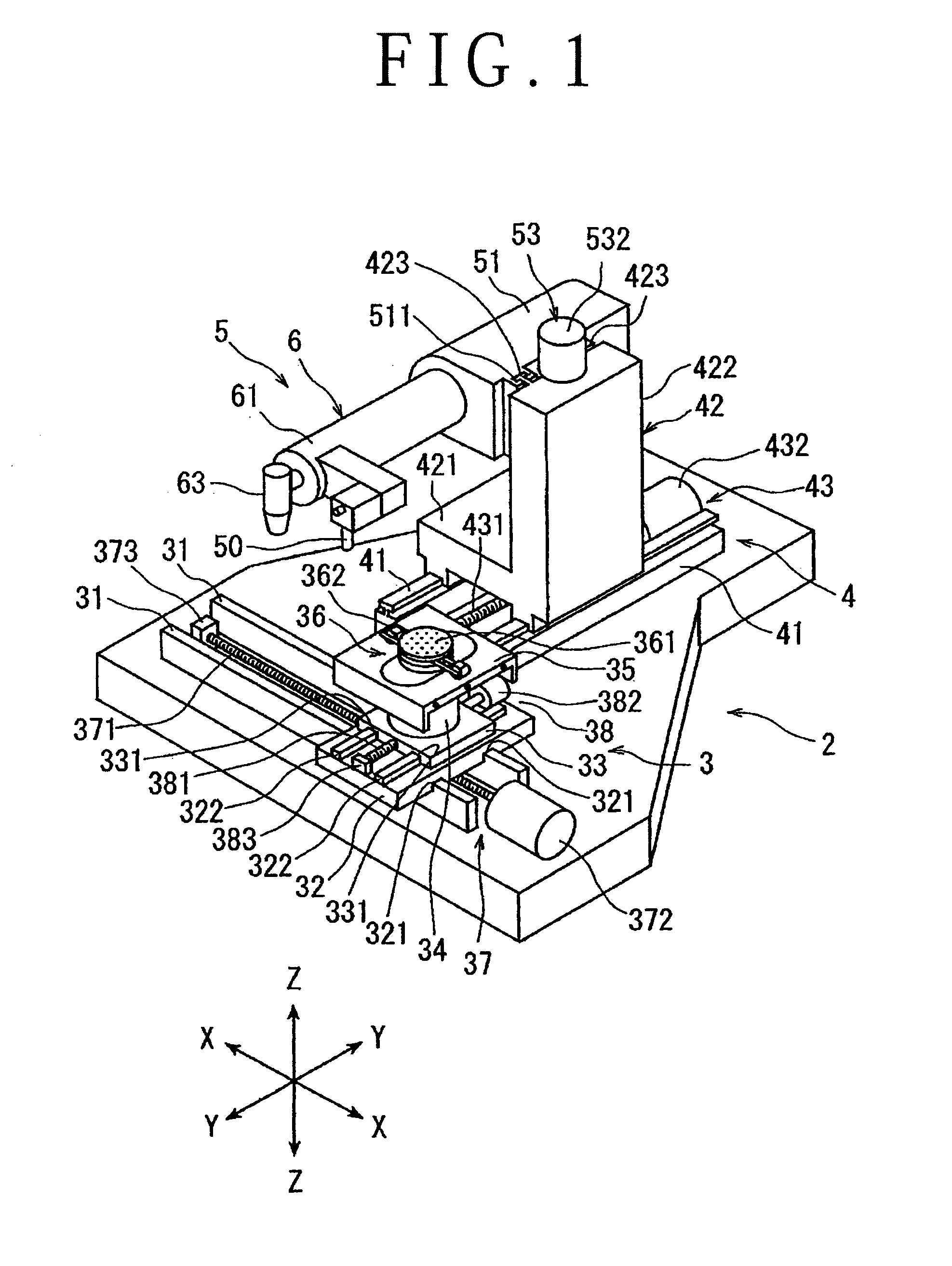
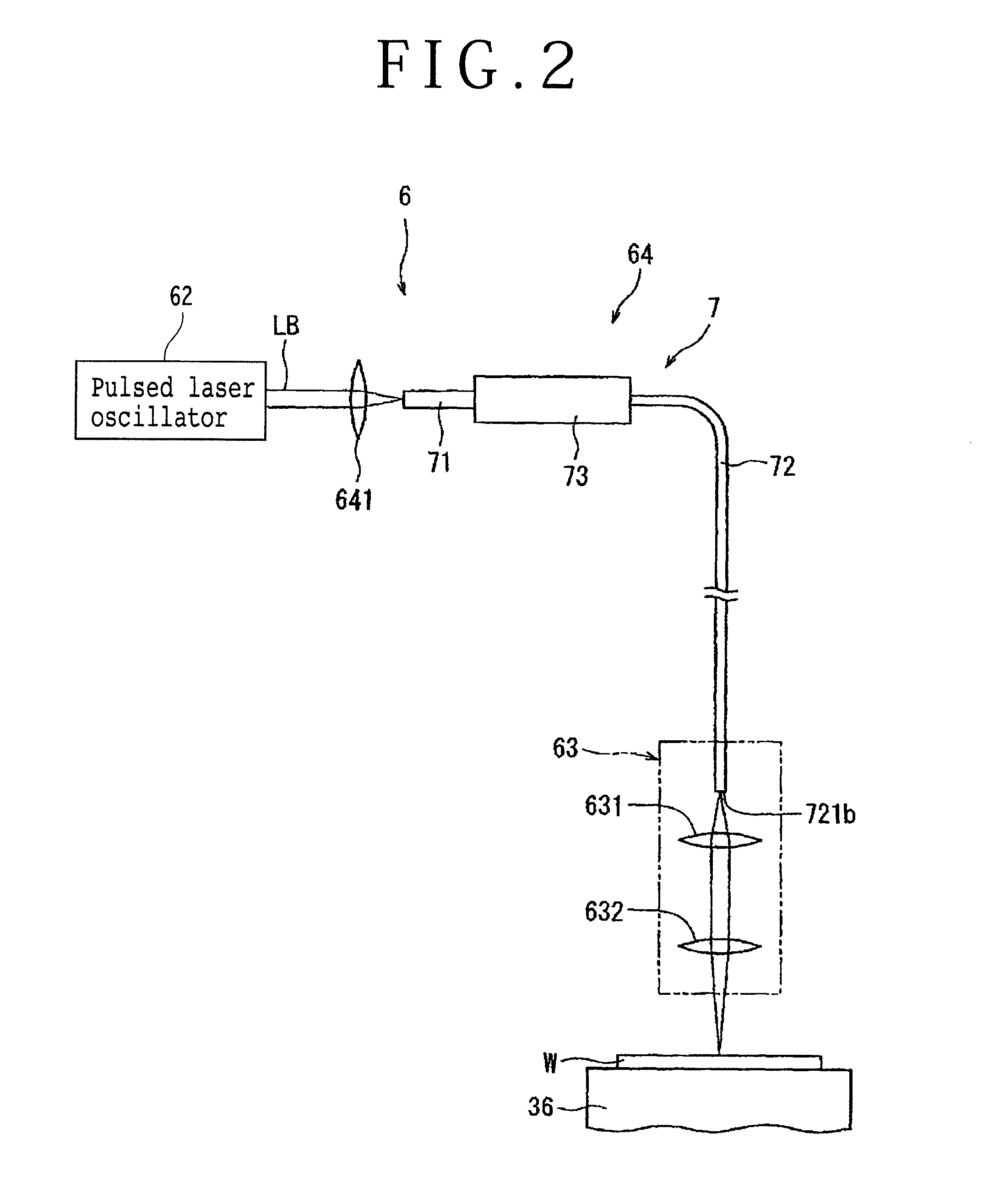
[0019]A preferred embodiment of the laser processing apparatus according to the present invention will now be described in detail with reference to the attached drawings. FIG. 1 is a perspective view of a laser processing apparatus according to a preferred embodiment of the present invention. The laser processing apparatus shown in FIG. 1 includes a stationary base 2, a chuck table mechanism 3 for holding a workpiece, the chuck table mechanism 3 being provided on the stationary base 2 so as to be movable in a feeding direction (X direction) shown by an arrow X, a laser beam applying unit supporting mechanism 4 provided on the stationary base 2 so as to be movable in an indexing direction (Y direction) shown by an arrow Y perpendicular to the X direction, and a laser beam applying unit 5 provided on the laser beam applying unit supporting mechanism 4 so as to be movable in a focal position adjusting direction (Z direction) shown by an arrow Z perpendicular to a holding surface of a c...
PUM
| Property | Measurement | Unit |
|---|---|---|
| diameter | aaaaa | aaaaa |
| diameter | aaaaa | aaaaa |
| diameter | aaaaa | aaaaa |
Abstract
Description
Claims
Application Information