Enhanced flash chip and method for packaging chip
a flash chip and enhanced technology, applied in the field of enhanced flash chips and packaging chips, can solve the problems of high complexity high cost, etc., and achieve the effects of high design cost, long design period, and high design complexity
- Summary
- Abstract
- Description
- Claims
- Application Information
AI Technical Summary
Benefits of technology
Problems solved by technology
Method used
Image

Examples
first embodiment
[0062]The first embodiment of the present application proposes an enhanced Flash chip which may comprise a FLASH and a RPMC packaged integrally.
[0063]In this embodiment of the present application, the FLASH and the RPMC may be independent chips. The FLASH may be selected to have different capacities to satisfy the requirements of various systems. The FLASH can reuse designed FLASH chips and hence there is no need redesign, greatly reducing the design period; the RPMC is provided with the function of replay protection monotonic counter and thus can be used independently.
[0064]In the enhanced Flash chip provided by the embodiments of the present application, the FLASH can comprise an independent controller and the RPMC can comprise an independent controller, respectively. In response to an external instruction, the FLASH and the RPMC may control the FLASH and the RPMC to receive and decode by the independent controllers, respectively. If the decoding is completed, corresponding operat...
second embodiment
[0076]Hereinafter, the enhanced Flash chip will be explained in detail by way of the second embodiment of the present application.
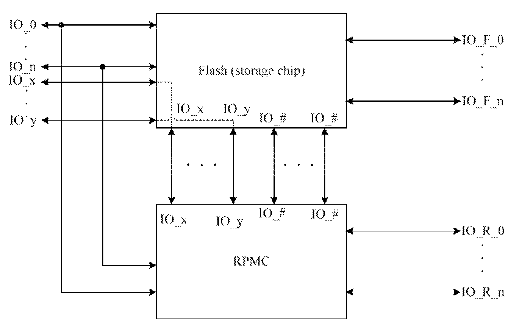
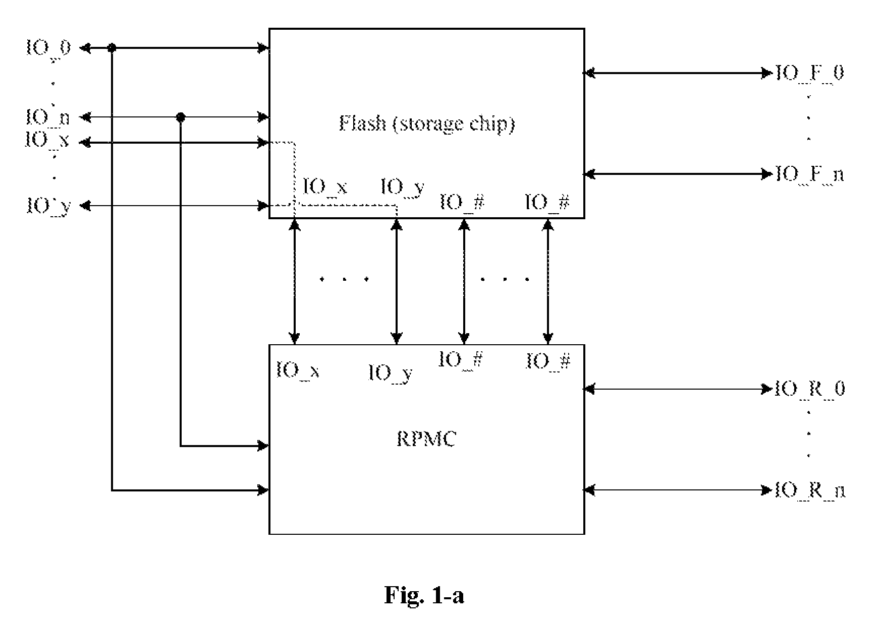
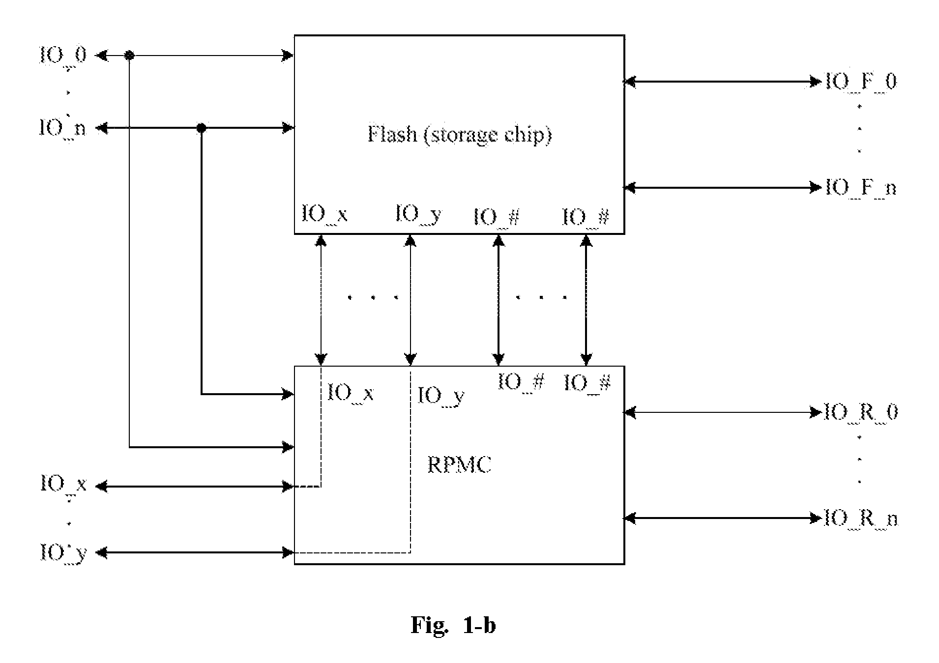
[0077]FIG. 1-a and FIG. 1-b show schematic diagrams of the logical connection of the enhanced Flash chip according to the second embodiment of the present application.
[0078]As could be seen from FIG. 1-a and FIG. 1-b, the enhanced Flash chip according to the embodiment of the present application may comprise a FLASH and a RPMC which are packaged integrally.
[0079]Herein, the FLASH and the RPMC each comprises a plurality of pins, and the same IO pins in the RPMC and the FLASH may be connected to the same set of external sharing pins.
[0080]The RPMC and the FLASH may receive an instruction from outside simultaneously and response correspondingly. The FLASH and the RPMC may farther comprise first internal IO pins and second internal IO pins, respectively, such that the first internal IO pins of the FLASH may be connected to the first internal IO pins of the RP...
third embodiment
[0149]Hereinafter, the specific method for packaging the chip will be explained by way of the third embodiment of the present application.
[0150]FIG. 3 shows a flow chart of the method for packaging chip according to the third embodiment of the present application. The method for packaging chip may comprise the following steps of:
[0151]Step 300: placing a FLASH and a RPMC (Replay Protection Monotonic Counter) to be packaged onto a chip carrier, the FLASH and the RPMC being mutually independent.
[0152]In this embodiment of the present application, the FLASH and the RPMC are substantially packaged integrally so as to obtain the enhanced Flash chip having the function of the RPMC, wherein the FLASH and the RPMC are mutually independent in the enhanced Flash chip.
[0153]First, the FLASH and the RPMC to be packaged may be placed onto the chip carrier. The chip carrier in this embodiment of the present application may correspond to Package in FIG. 2.
[0154]Preferably, Step 300 may comprise: p...
PUM
 Abstract
Description
Claims
Application Information
 - R&D Engineer
- R&D Manager
- IP Professional
- Industry Leading Data Capabilities
- Powerful AI technology
- Patent DNA Extraction
Browse by: Latest US Patents, China's latest patents, Technical Efficacy Thesaurus, Application Domain, Technology Topic.
© 2024 PatSnap. All rights reserved.Legal|Privacy policy|Modern Slavery Act Transparency Statement|Sitemap