

Voltage converting device
a voltage conversion device and voltage technology, applied in logic circuits, pulse techniques, instruments, etc., can solve problems such as more power consumption, and achieve the effect of reducing power consumption and fewer conversion circuit stages
- Summary
- Abstract
- Description
- Claims
- Application Information
AI Technical Summary
Benefits of technology
Problems solved by technology
Method used
Image

Examples
Embodiment Construction
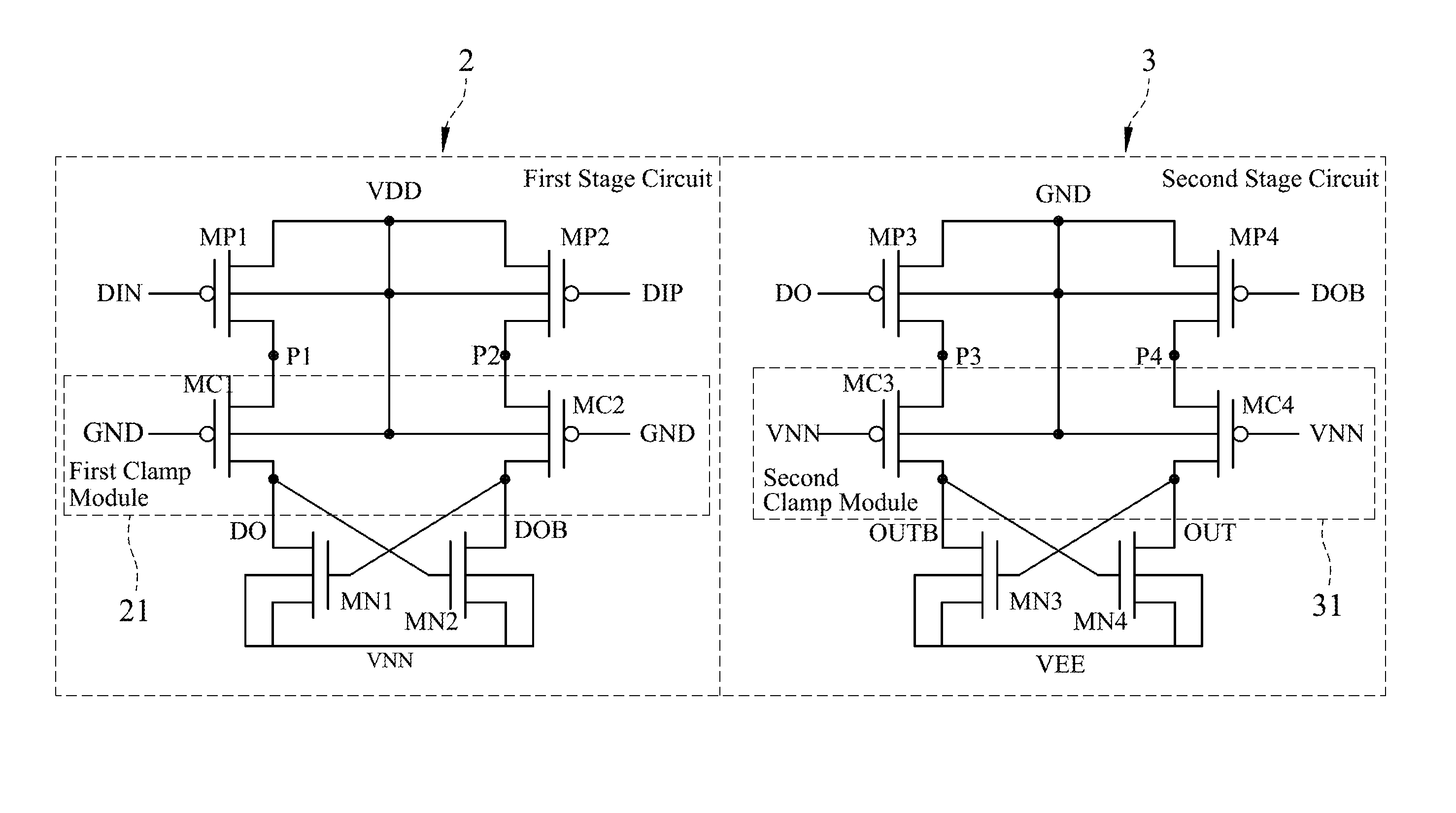
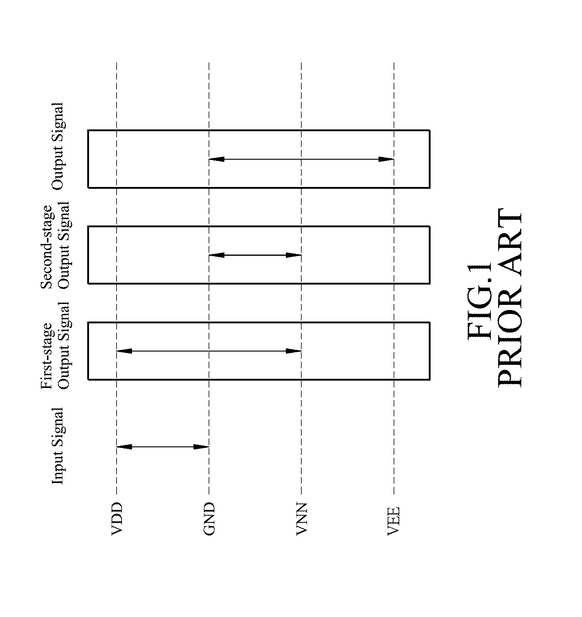
[0025]Referring to FIG. 3 and FIG. 4, the preferred embodiment of the voltage converting device according to this invention is shown to include a first stage circuit 2 and a second stage circuit 3, and receives a first voltage VDD, a second voltage GND lower than the first voltage VDD, a third voltage VNN lower than the second voltage GND, and a fourth voltage VEE lower than the third voltage VNN.
[0026]The first stage circuit 2 converts a differential voltage, which ranges between the first voltage VDD and the second voltage GND and includes complementary first and second single-ended voltages DIP, DIN, to a first stage differential output signal having a magnitude ranging between the first voltage VDD and the third voltage VNN. The first stage differential output signal includes complementary first and second single-ended output voltages DO, DOB.
[0027]The first stage circuit 2 includes input transistors MP1, MP2, output transistors MN1, MN2, and a first-stage clamp module 21.
[0028]...
PUM
 Abstract
Description
Claims
Application Information