
Multiple register memory access instructions, processors, methods, and systems

a multi-register memory and instruction technology, applied in the field of processors, can solve the problems of increasing the area or the footprint occupied by the register on the die, and increasing the width of the register

Active Publication Date: 2016-08-23
INTEL CORP
View PDF15 Cites 6 Cited by
  • Summary
  • Abstract
  • Description
  • Claims
  • Application Information

AI Technical Summary

Problems solved by technology

However, one possible drawback to increasing the width of the registers is an increase in the area or footprint occupied by the registers on die.
Another possible drawback to such an increase in the width of the registers is a corresponding increase in the amount of state, context, or other data stored in the registers that needs to be moved to and from the registers (e.g., saved and restored) on context switches, power mode state saves, and like transitions.

Method used


Image

  • Multiple register memory access instructions, processors, methods, and systems
  • Multiple register memory access instructions, processors, methods, and systems
  • Multiple register memory access instructions, processors, methods, and systems

Examples


example embodiments

[0133]The following examples pertain to further embodiments. Specifics in the examples may be used anywhere in one or more embodiments.

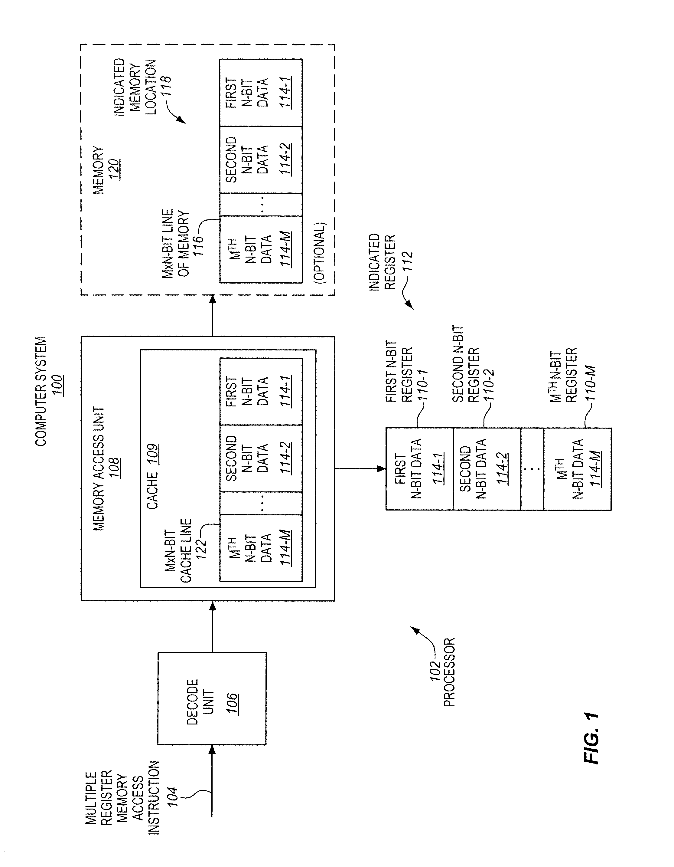
[0134]Example 1 is a processor that includes a plurality of N-bit registers. The processor also includes a decode unit to receive a multiple register memory access instruction. The multiple register memory access instruction is to indicate a memory location and is to indicate a register. The processor also includes a memory access unit coupled with the decode unit and with the plurality of the N-bit registers. The memory access unit is to perform a multiple register memory access operation in response to the multiple register memory access instruction. The multiple register memory access operation is to involve N-bit data, in each of the plurality of the N-bit registers that are to comprise the indicated register. The multiple register memory access operation is also to involve different corresponding N-bit portions of an M×N-bit line of memory, that...


PUM


Abstract

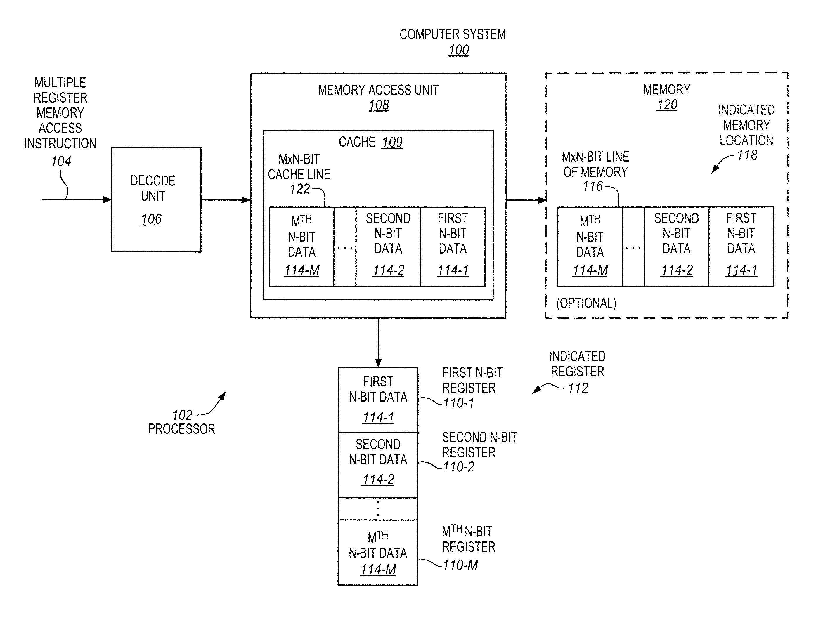
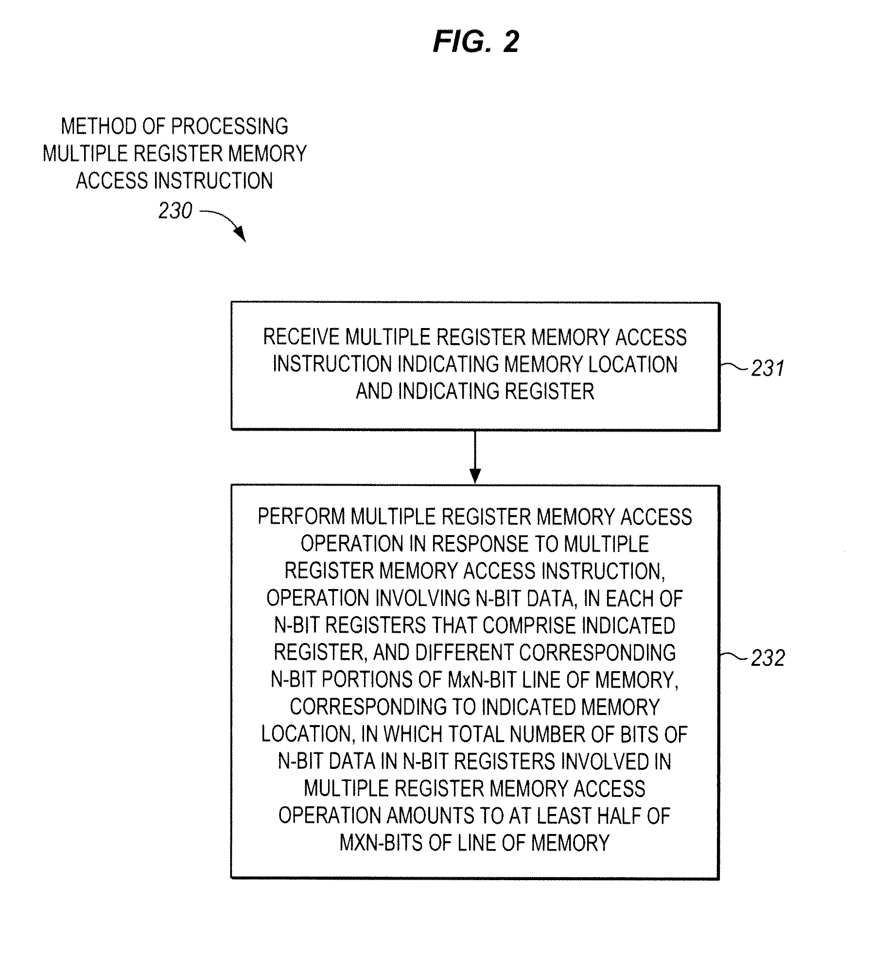
A processor includes N-bit registers and a decode unit to receive a multiple register memory access instruction. The multiple register memory access instruction is to indicate a memory location and a register. The processor includes a memory access unit coupled with the decode unit and with the N-bit registers. The memory access unit is to perform a multiple register memory access operation in response to the multiple register memory access instruction. The operation is to involve N-bit data, in each of the N-bit registers comprising the indicated register. The operation is also to involve different corresponding N-bit portions of an M×N-bit line of memory corresponding to the indicated memory location. A total number of bits of the N-bit data in the N-bit registers to be involved in the multiple register memory access operation is to amount to at least half of the M×N-bits of the line of memory.

Description

BACKGROUND[0001]1. Technical Field[0002]Embodiments described herein generally relate to processors. In particular, embodiments described herein generally relate to accessing data in memory with processors.[0003]2. Background Information[0004]Many processors have Single Instruction, Multiple Data (SIMD) architectures. In SIMD architectures, a packed data instruction, vector instruction, or SIMD instruction may operate on multiple data elements (e.g., multiple pairs of data elements) concurrently or in parallel. Multiple data elements may be packed within a register or memory location as packed data. In packed data, the bits of the register or other storage location may be logically divided into a sequence of data elements. For example, a 64-bit wide packed data register may have two packed 32-bit data elements, four packed 16-bit data elements, or eight packed 8-bit data elements. The processor may have parallel execution hardware responsive to the packed data instruction to perform...

Claims


Application Information

Patent Timeline
Patent Type & Authority Patents(United States)
IPC IPC(8): G06F9/04G06F9/30
CPCG06F9/30043G06F9/30109G06F9/30163G11C7/1036
Inventor HINTON, GLENNTOLL, BRETSINGHAL, RONAK
Owner INTEL CORP
Learn More