Scan driving circuit and display panel

a driving circuit and display panel technology, applied in the direction of instruments, static indicating devices, etc., can solve the problems of line breakage or signal delay, the design of narrow bezels cannot be realized, and the width of the fan-out lines is so small, so as to reduce the layout space of the fan-out lines

Active Publication Date: 2016-09-06
TCL CHINA STAR OPTOELECTRONICS TECH CO LTD
View PDF12 Cites 2 Cited by
  • Summary
  • Abstract
  • Description
  • Claims
  • Application Information

AI Technical Summary

Benefits of technology

[0004]The main technique problem solved by the present invention is to provide a scan driving circuit and display panel, which reduces an amount of the gate driving chips in the fan-out block and the layout space of the fan-out line such that the design of narrow bezel can be realized.
[0025]The beneficial effect of the present invention is: different from the conventional technique, the scan driving circuit and the display panel of the present invention drives a plurality of scan lines by one fan-out line through connecting the control lines at least one of the switches of each of the switch sets individually, and connecting the fan-out line to the scan lines through the switch sets, so as to turn on the scan lines separately under control of the fan-out line and the control lines, such that an amount of the gate driving chips in the fan-out block and the layout space of the fan-out line can be reduced, and therefore the design of a narrow bezel display panel could be reached.

Problems solved by technology

The amount of the gate IC corresponding to the fan-out lines is increased when the scan lines are driven by single gate driving method, such that the area occupied by the fan-out block of the display panel is increased and therefore the design of narrow bezel cannot be realized.
Besides, the width of the fan-out line corresponding to each scan line would be reduced as the resolution of the display panel getting higher if the area of the fan-out block remains the same, such that the line width of the fan-out lines is so small that the problem of line broken or signal delay would be occurred.

Method used


Image

  • Scan driving circuit and display panel
  • Scan driving circuit and display panel
  • Scan driving circuit and display panel

Examples


first embodiment

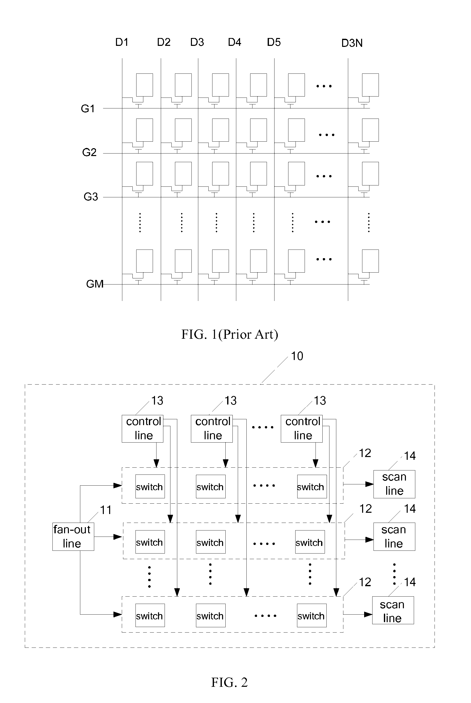
[0033]FIG. 2 is a structure schematic diagram of a scan driving circuit according to the present invention. As shown in FIG. 2, the scan driving circuit comprises a plurality of scan driving units 10. Each of the scan driving units 10 comprises a fan-out line 11, a plurality of switch sets 12, a plurality of control lines 13 and a plurality of scan lines 14, wherein an amount of the switch sets 12, the amount of switches in each of the switch sets 12, the amount of the control lines 13 and the amount of the scan lines 14 are the same. Wherein, the control line 13 in each of the scan driving units 10 is connected to each other.

[0034]The control lines 13 are connected to at least one of the switches of each of the switch sets 12 individually; the fan-out line 11 is connected to the scan lines 14 through the switch sets 12, such that the scan lines 14 are turned on separately under control of the fan-out line 11 and the control lines 13. Wherein, the switch sets 12 are correspondence t...

second embodiment

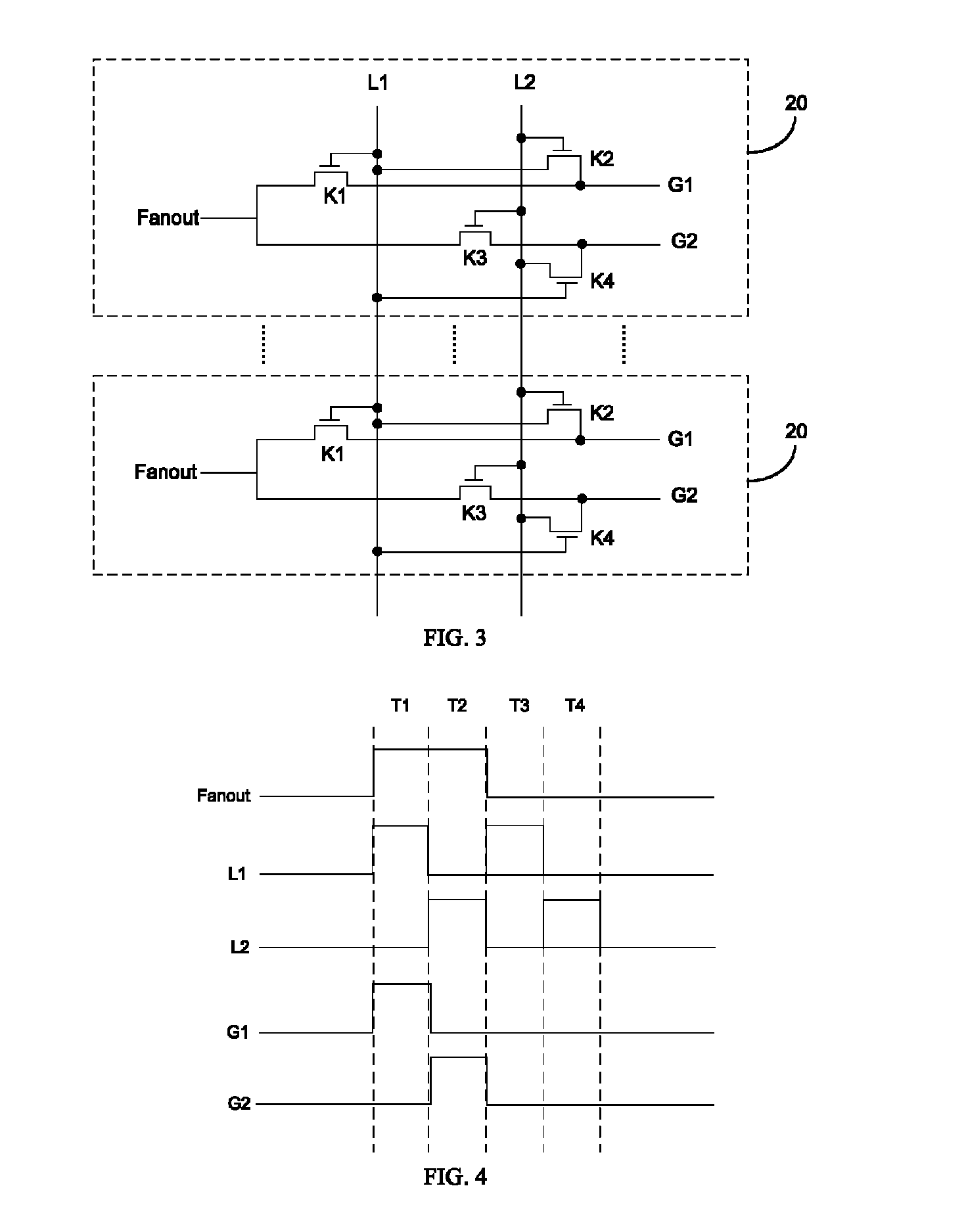
[0035]FIG. 3 is a circuit diagram of a scan driving circuit according to the present invention. As shown in FIG. 3, the scan driving circuit comprises a plurality of scan driving units 20, and each scan driving unit 20 comprises a fan-out line Fanout, a first TFT switch K1, a second TFT switch K2, a third TFT switch K3, a fourth TFT switch K4, a first control line L1, a second control line L2, a first scan line G1 and a second scan line G2.

[0036]Wherein, the amount of the switch sets, the amount of switches in each of the switch sets, the amount of the control lines and the amount of the scan lines are the same, i.e., 2.

[0037]Wherein, a first switch set is formed by the first TFT switch K1 and the second TFT switch K2, and a second switch set is formed by the third TFT switch K3 and the fourth TFT switch K4.

[0038]In the first switch set, the first control line L1 is connected to a gate electrode of the first TFT switch K1 and a source electrode of the second TFT switch K2, and the s...

third embodiment

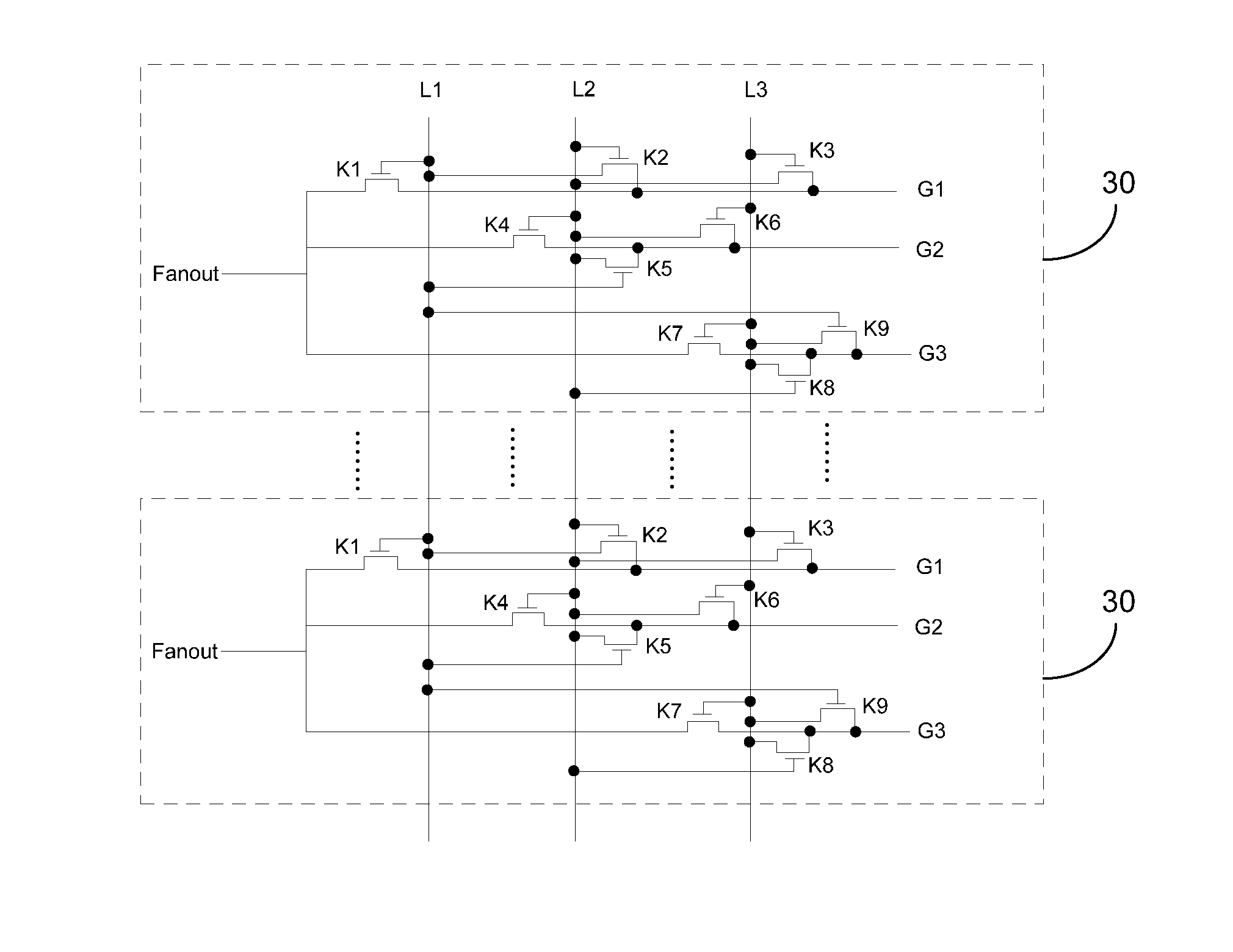
[0045]FIG. 5 is a circuit diagram of a scan driving circuit according to the present invention. As shown in FIG. 5, the scan driving circuit comprises a plurality of scan driving units 30. Each scan driving unit 30 comprises a fan-out line Fanout, a first TFT switch K1, a second TFT switch K2, a third TFT switch K3, a fourth TFT switch K4, a fifth TFT switch K5, a sixth TFT switch K6, a seventh TFT switch K7, an eighth TFT switch K8, a ninth TFT switch K9, a first control line L1, a second control line L2, a third control line L3, a first scan line G1, a second scan line G2 and a third scan line G3. Wherein, the first control lines L1 in every scan driving unit 30 is connected to each other, the second control line L2 in every scan driving unit 30 is connected to each other, and the third control line L3 in every scan driving unit 30 is connected to each other.

[0046]Wherein, the amount of the switch sets, the amount of the switches in each of the switch sets, the amount of the contr...


PUM


Abstract

The present invention provides a scan driving circuit and display panel. The scan driving circuit comprises a plurality of scan driving units, each of which comprises a fan-out line, a plurality of switch sets, a plurality of control lines and a plurality of scan lines. The control lines are connected to at least one of the switches of each of the switch sets individually and the fan-out line is connected to the scan lines through the switch sets, such that the scan lines are turned on separately under control of the fan-out line and the control lines. By the above mentioned solution, the present invention drives a plurality of scan lines by one fan-out line such that an amount of the gate driving chips in the fan-out block and the layout space of the fan-out line can be reduced.

Description

FIELD OF THE INVENTION[0001]The present invention relates to a technique field of liquid crystal display, and more particularly to a scan driving circuit and display panel.BACKGROUND OF THE INVENTION[0002]FIG. 1 is a structural schematic diagram of a display panel in the prior art. As shown in FIG. 1, each pixel in the display panel is controlled by a gate line and a data line. A display panel of which the resolution is M*N should have M scan lines Gn (n=1, 2, . . . , M) and 3N data lines Dn (n=1, 2, . . . , 3N).[0003]As the resolution of the display panel getting higher, the amount of the gate line and the amount of the fan-out line corresponding to the gate lines increase as well. The amount of the gate IC corresponding to the fan-out lines is increased when the scan lines are driven by single gate driving method, such that the area occupied by the fan-out block of the display panel is increased and therefore the design of narrow bezel cannot be realized. Besides, the width of the...

Claims


Application Information

Patent Timeline
Patent Type & Authority Patents(United States)
IPC IPC(8): G09G3/36
CPCG09G3/3677G09G2300/0426G09G2310/08G09G2320/0223
Inventor GUO, JINBOWANG, JINJIECHEN, CAIQIN
Owner TCL CHINA STAR OPTOELECTRONICS TECH CO LTD
Why Eureka
Try Eureka