
Power converter

a power converter and converter technology, applied in the field of power converters, can solve the problems of surge problem becoming significant for the inability to use a 2-in-1 semiconductor device, and the surge problem so as to prevent the surge of a 1-in-1 semiconductor device, prevent the surge voltage, boost or reduce the effect of voltag

Active Publication Date: 2017-03-14
DENSO CORP
View PDF12 Cites 1 Cited by
  • Summary
  • Abstract
  • Description
  • Claims
  • Application Information

AI Technical Summary

Benefits of technology

[0007]A power converter disclosed herein uses an electric current flowing in a high potential side terminal connected to an upper arm circuit and an electric current flowing in a low potential side terminal connected to a lower arm circuit, to prevent a surge voltage from being generated. Specifically, a wiring connected to the high potential side terminal is disposed parallel to a wiring connected to the low potential side terminal, and electric currents flowing in both wirings are made opposite to each other, so that magnetic fields generated by the current supply cancel each other out, thereby preventing mutual inductance from occurring. By preventing the mutual inductance from occurring, a surge is prevented from occurring in the semiconductor device as a result. Notably, in a power converter having an upper arm circuit and a lower arm circuit, theoretically, electric currents do not flow in the upper arm circuit and the lower arm circuit at the same time. However, when the upper arm circuit (or the lower arm circuit) is switched from on state to off state, there is a period during which the electric currents transiently flow both in the upper arm circuit and the lower arm circuit at the same time. The power converter disclosed herein uses the period during which the electric currents transiently flow both in the upper arm circuit and the lower arm circuit at the same time, thereby preventing mutual inductance from occurring, and then preventing a surge from occurring.
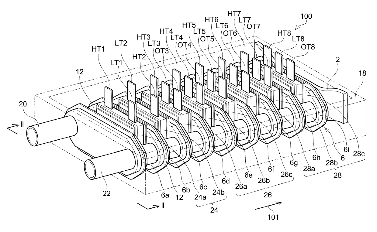
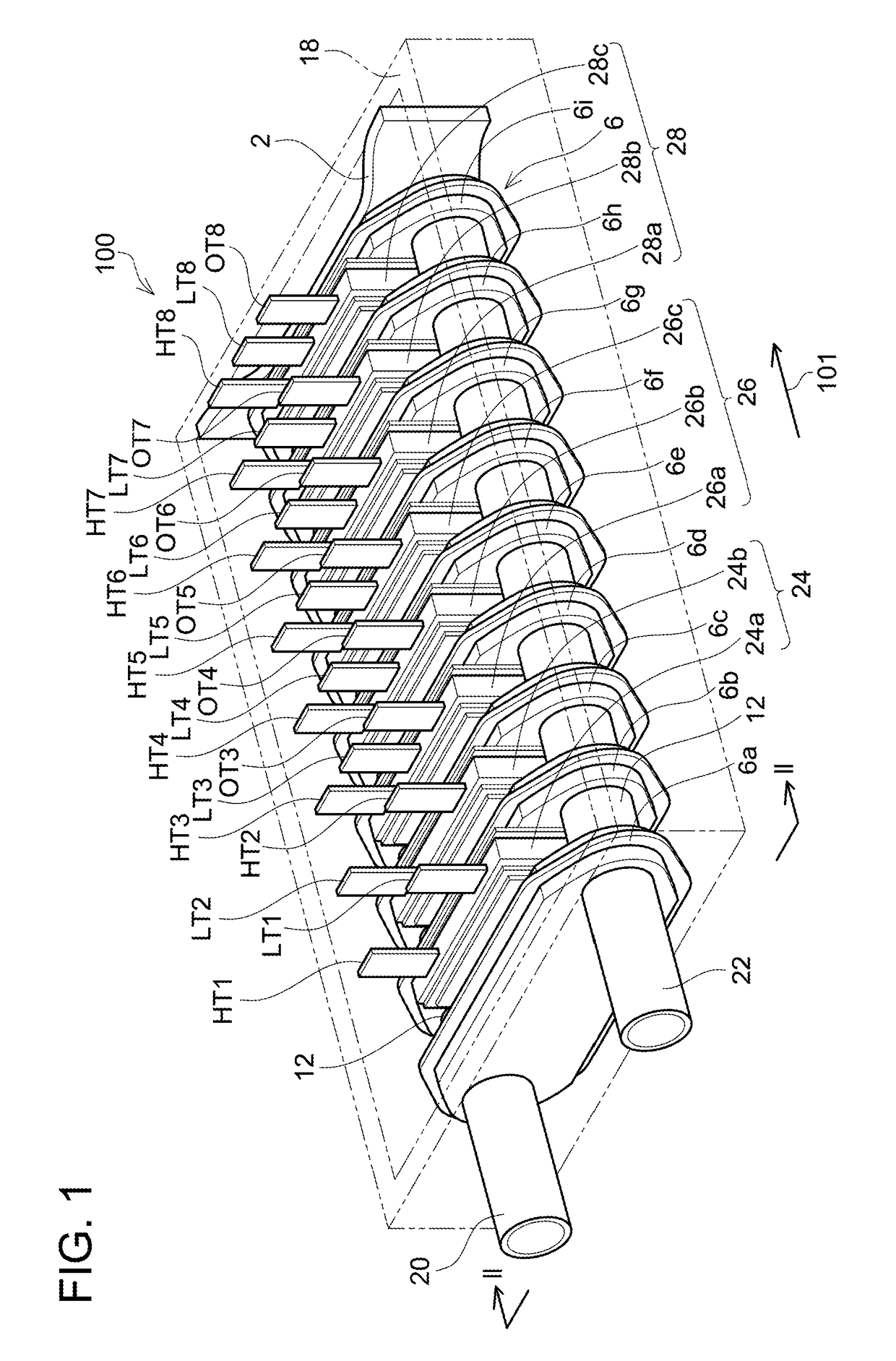
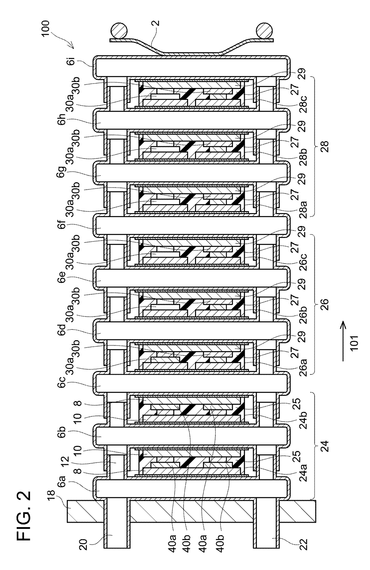
[0010]In the above power converter, when viewed along the stacking direction 101, a position of the first high potential side terminal HT1 in the direction 103 is matched with a position of the second low potential side terminal LT2 in the direction 103. As a result, in the direction 103, a position where the wiring L1 is connected to the first high potential side terminal HT1 is matched with a position where the wiring L2 is connected to the second low potential side terminal LT2. When a transistor of the semiconductor device 24a (or a transistor of the semiconductor device24b) is switched from on state to off state, opposite-direction currents transiently flow in the wirings L1 and L2, so that magnetic fields generated by the current supply cancel each other out. As a result, mutual inductance can be reduced, so that surge voltages can be prevented from being generated in the semiconductor devices 24a and 24b.

Problems solved by technology

In addition, there may be a case where a 2-in-1 semiconductor device cannot be used due to having to connect to a reactor configuring a converter.
In particular, in a power converter in which each of the upper arm circuit and the lower arm circuit is switched on or off at high frequency, the surge problem becomes significant for a 1-in-1 semiconductor device because the 1 in 1 semiconductor device has a larger number of input and output terminals than a number of input and output terminals an N-in-1 semiconductor device has.

Method used


Image

  • Power converter
  • Power converter
  • Power converter

Examples


first embodiment

[0028]Referring to FIGS. 1 to 3, a power converter 100 will be described. In FIG. 1, a housing 18 of the power converter 100 is indicated by imaginary lines, and in FIG. 2, only a portion of the housing 18 is illustrated. In the following descriptions, alphabets in reference numerals of components may be omitted when the components have a substantially same function.

[0029]As illustrated in FIGS. 1 and 2, the power converter 100 has a voltage converter circuit 24, a first inverter circuit 26, and a second inverter circuit 28. As illustrated in FIG. 3, the power converter 100 is used for driving two motors 50 and 52. The motors 50 and 52 are used for driving an electric vehicle, for instance. Specifically, the power converter 100 includes the voltage converter circuit 24 which is a chopper type and boosts a voltage of a power supply 56, the first inverter circuit 26 which converts a direct current power after the boosting to an alternate current power, and the second inverter circuit ...

second embodiment

[0055]Referring to FIGS. 5 to 7, a power converter 200 will be described. The power converter 200 is a modification of the power converter 100, and a voltage converter circuit 224 differs in structure from the voltage converter circuit 24 of the power converter 100. The first inverter circuit 26 and the second inverter circuit 28 have the same structure as those of the power converter 100. Thus, in FIGS. 6 and 7, only the voltage converter circuit 224 is illustrated, and the inverter circuits are omitted. The same components of the power converter 200 as those of the power converter 100 are indicated by the same reference numerals or reference numerals having identical last two digits, and the description thereof may hereinafter be omitted.

[0056]The voltage converter circuit 224 has semiconductor devices 24a and 24b, and a semiconductor device 24c. The semiconductor device 24c has substantially a same structure as those of the semiconductor devices 24a and 24b. As illustrated in FIG...

third embodiment

[0061]Referring to FIG. 8, a power converter 300 will be described. The power converter 300 is a modification of the power converters 100 and 200, and a voltage converter circuit 324 differs in structure from the voltage converter circuit 24 of the power converter 100 and the voltage converter circuit 224 of the power converter 200. Inverter circuits in the power converter 300 have the same structure as those of the power converters 100 and 200. Thus, in FIG. 8, only the voltage converter circuit 324 is illustrated, and the inverter circuits are omitted. The same components of the power converter 300 as those of the power converters 100 and 200 are indicated by the same reference numerals or reference numerals having identical last two digits, and the description thereof may hereinafter be omitted. FIG. 8 illustrates only a circuit diagram of the voltage converter circuit 324.

[0062]As illustrated in FIG. 8, the voltage converter circuit 324 has one upper arm circuit 324a, and three ...


PUM


Abstract

In a power converter, a plurality of semiconductor devices and a plurality of cooling plates are stacked. The plurality of semiconductor devices includes a first-first sealed semiconductor device, a second-first sealed semiconductor device, and a plurality of second sealed semiconductor devices. The first-first sealed semiconductor device has a first high potential side terminal, and a first low potential side terminal. The second-first sealed semiconductor device has a second high potential side terminal, and a second low potential side terminal. When viewed along a stacking direction, the first high potential side terminal is disposed to overlap with the second low potential side terminal.

Description

CROSS-REFERENCE TO RELATED APPLICATION[0001]This application claims priority based on Japanese Patent Application No. 2015-038627, filed on Feb. 27, 2015, the entire contents of which are hereby incorporated by reference into the present disclosure.TECHNICAL FIELD[0002]The present disclosure relates to a power converter. More specifically, present disclosure discloses a technique relating to a power converter in which semiconductor devices are stacked alternately with cooling plates.DESCRIPTION OF RELATED ART[0003]A power converter in which semiconductor devices are stacked alternately with cooling plates has been developed, and is disclosed in Japanese Patent Application Publication No. 2013-93343. Hereinafter, Japanese Patent Application Publication No. 2013-93343 is referred to as Patent Literature 1. In the power converter in Patent Literature 1, a semiconductor element configuring an upper arm circuit and a semiconductor element configuring a lower arm circuit are incorporated ...

Claims


Application Information

Patent Timeline
Patent Type & Authority Patents(United States)
IPC IPC(8): H01L23/367H01L25/065H01L23/31H02M7/5387H01L25/11H01L23/473H02M7/00H01L23/40
CPCH01L23/31H01L23/40H01L23/473H01L25/117H02M7/003H01L23/4012H01L23/051H01L23/3107
Inventor OHNO, HIROTAKA
Owner DENSO CORP
Learn More