
Solid hard disk and charging/discharging control method for flash chip

a control method and flash chip technology, applied in the field of storage technologies, can solve the problems of reducing abrasion achieve the effects of prolonging the service life of the flash chip, reducing the times of charging/discharging, and avoiding repeated charging/discharging

Active Publication Date: 2017-03-28
RAMAXEL TECH SHENZHEN
View PDF10 Cites 0 Cited by
  • Summary
  • Abstract
  • Description
  • Claims
  • Application Information

AI Technical Summary

Benefits of technology

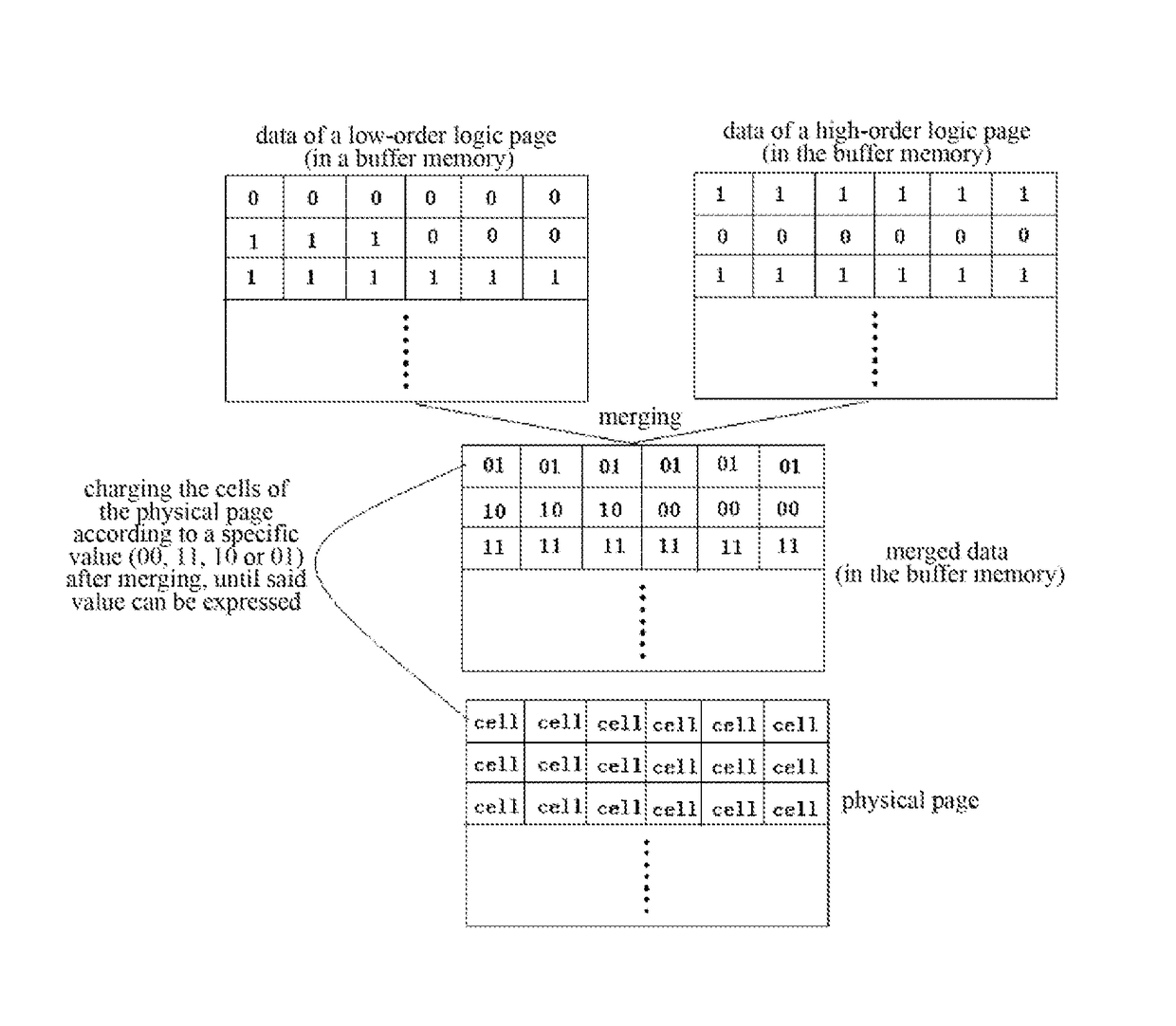
The present invention provides a solid hard disk and a charging / discharging control method for a flash chip. The technical effect of this invention is to avoid repeated charging / discharging of the multi-layer memory cell, reduce the times of charging / discharging and abrasion of the flash chip, and prolong the service life of the flash chip. This is achieved by mapping a same physical page to two mutually coupled logic pages and writing data to both pages simultaneously, so that a voltage state of the multi-layer memory cell is expressed as a numerical value of the merged data. Compared with the prior art method, the present invention reduces the times of charging / discharging and abrasion of the flash chip and prolongs its service life.

Problems solved by technology

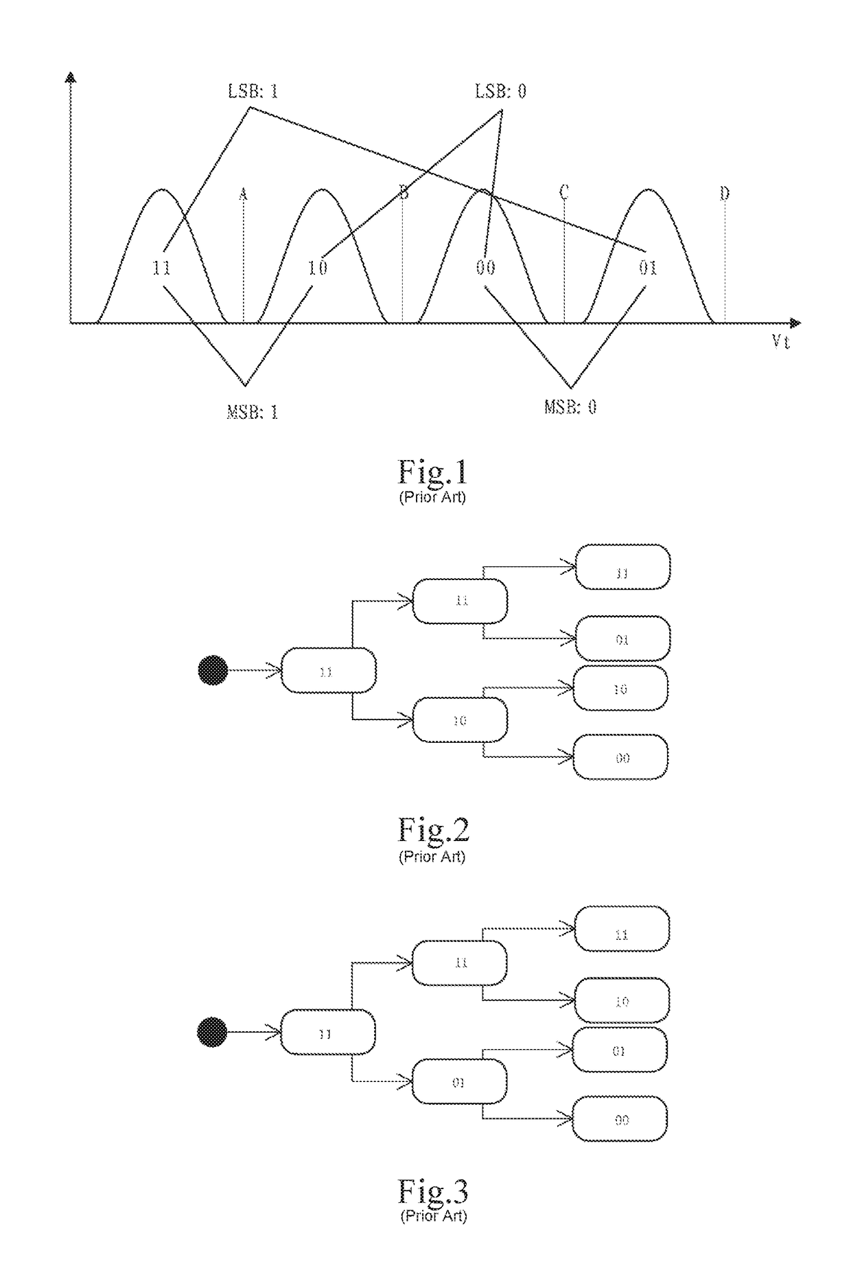
In this way, since the LSB and MSB of an MLC-type flash chip share a physical memory cell, when the LSB or MSB is being programmed, the physical memory cell needs to be charged or discharged, and the times of frequent charging / discharging reduce the times of erasure of the MLC-type flash chip, resulting in abrasion of the flash chip and reducing the service life of the flash chip.
To sum up, the practical application of the existing charging / discharging control methods for MLC NAND-type flash chips is obviously inconvenient and deficient, thus it is necessary to make an improvement.

Method used


Image

  • Solid hard disk and charging/discharging control method for flash chip
  • Solid hard disk and charging/discharging control method for flash chip
  • Solid hard disk and charging/discharging control method for flash chip

Examples


Embodiment Construction

[0044]To clarify the object, technical solutions and advantages of the present invention, the present invention will be further explained in detail hereinafter with reference to the accompanying drawings and embodiments. It should be appreciated that the specific embodiments described herein are merely intended to illustrate the present invention but are not limited thereto.

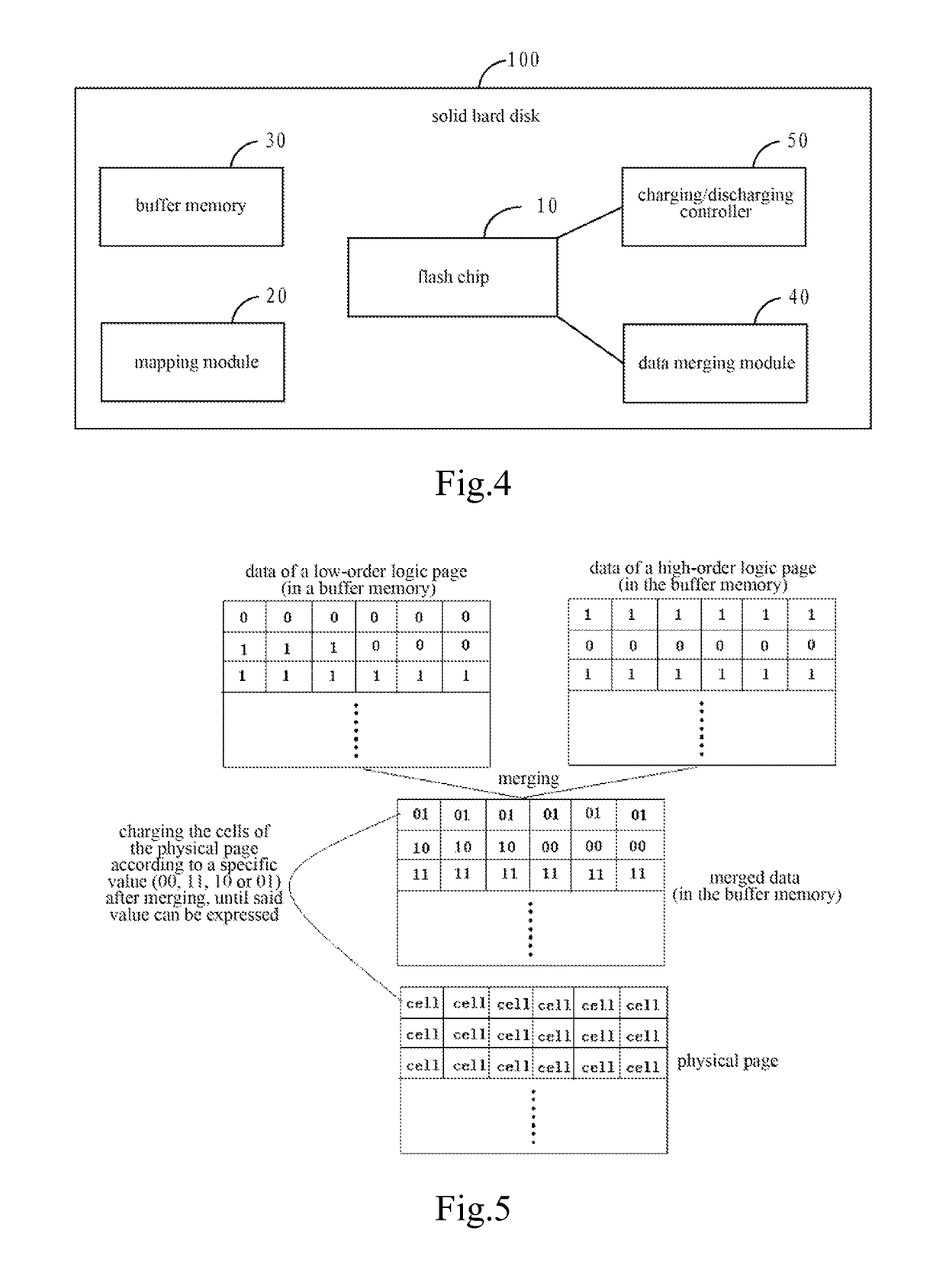
[0045]As shown in FIG. 4, a solid hard disk 100 according to the present invention comprises a plurality of flash chips 10, each of which has a plurality of physical pages, each physical page comprising a plurality of multi-layer memory cells. The solid hard disk 100 further comprises a mapping module 20, a buffer memory 30, a data merging module 40 and a charging / discharging controller 50, wherein the data merging module 40 and the charging / discharging controller 50 are electrically connected to the multi-layer memory cells of the flash chip 10.

[0046]The mapping module 20 is adapted to map a same physical page t...


PUM


Abstract

A method comprises steps of mapping a same physical page to two mutually coupled logic pages, one logic page being formed by mapping the least significant bit on the physical page, and the other logic page being formed by mapping the most significant bit on the physical page; buffering write data in a buffer memory, and merging the data, which is corresponding to the two mutually coupled logic pages, in the buffer memory into a piece of data corresponding to the physical page according to the mapping relationship between the physical page and the two mutually coupled logic pages; and performing charging / discharging control for the multi-layer memory cell of the physical page according to the merged data, so that a voltage state of the multi-layer memory cell is expressed as a numerical value of the merged data.

Description

TECHNICAL FIELD[0001]The present invention relates to the field of storage technologies, and particularly to a solid hard disk and a charging / discharging control method for a flash chip.BACKGROUND ART[0002]NAND-type flash memories can be divided into SLC (Single-Level Cell) NAND-type flash memories and MLC NAND-type flash memories according to the digits that can be stored in each memory cell.[0003]Each memory cell of an SLC NAND-type flash chip may have two states: a high voltage state and a low voltage state, which represent the data 0 and 1, respectively. Such a memory cell may represent a data bit. A plurality of physical memory cells form a physical page, which may represent a same number of bits, namely a logic page.[0004]Each memory cell of an MLC NAND-type flash chip may have four voltage states. MLC represents different data according to different voltage values. FIG. 1 is a schematic view illustrating voltage distribution of a memory cell of an MLC NAND-type flash chip, wh...

Claims


Application Information

Patent Timeline
Patent Type & Authority Patents(United States)
IPC IPC(8): G11C11/56
CPCG11C11/5628G11C2211/5648
Inventor JIN, MING
Owner RAMAXEL TECH SHENZHEN
Learn More