Method and apparatus for manufacturing optical display device

a technology of optical display and manufacturing method, which is applied in the direction of instruments, other domestic objects, transportation and packaging, etc., can solve the problems cycle time, and high manufacturing speed of optical film sheets, and achieve the effect of high laminating accuracy

Inactive Publication Date: 2017-05-09
NITTO DENKO CORP
View PDF13 Cites 0 Cited by
  • Summary
  • Abstract
  • Description
  • Claims
  • Application Information

AI Technical Summary

Benefits of technology

[0016]An aim of the present invention is to provide a method and an apparatus for manufacturing an optical display device with high laminating accuracy, as mentioned above.
[0035]In the first embodiment, the second, the fifth and the seventh steps are preferably configured to operate a carrier film feeding means 8 comprising forward / reverse feed rollers 80, 81 arranged at upstream and at downstream of the tip-end 61 of the movable peeling member 60 to wind or unwind the carrier film 2 without slacking.

Problems solved by technology

Roll length of such an optical film laminate is about 900 m. However, manufacturing speed i.e., cycle time for such middle- or small-sized liquid-crystal display device is required to be two times higher than that for a large liquid-crystal display device, and laminating accuracy for an optical film sheet, such as a polarizing film supported on a carrier film, to be laminated to a liquid-crystal panel LC is also very severe.

Method used


Image

  • Method and apparatus for manufacturing optical display device
  • Method and apparatus for manufacturing optical display device
  • Method and apparatus for manufacturing optical display device

Examples


Embodiment Construction

Overview of a Method and an Apparatus for Manufacturing an Optical Display Device

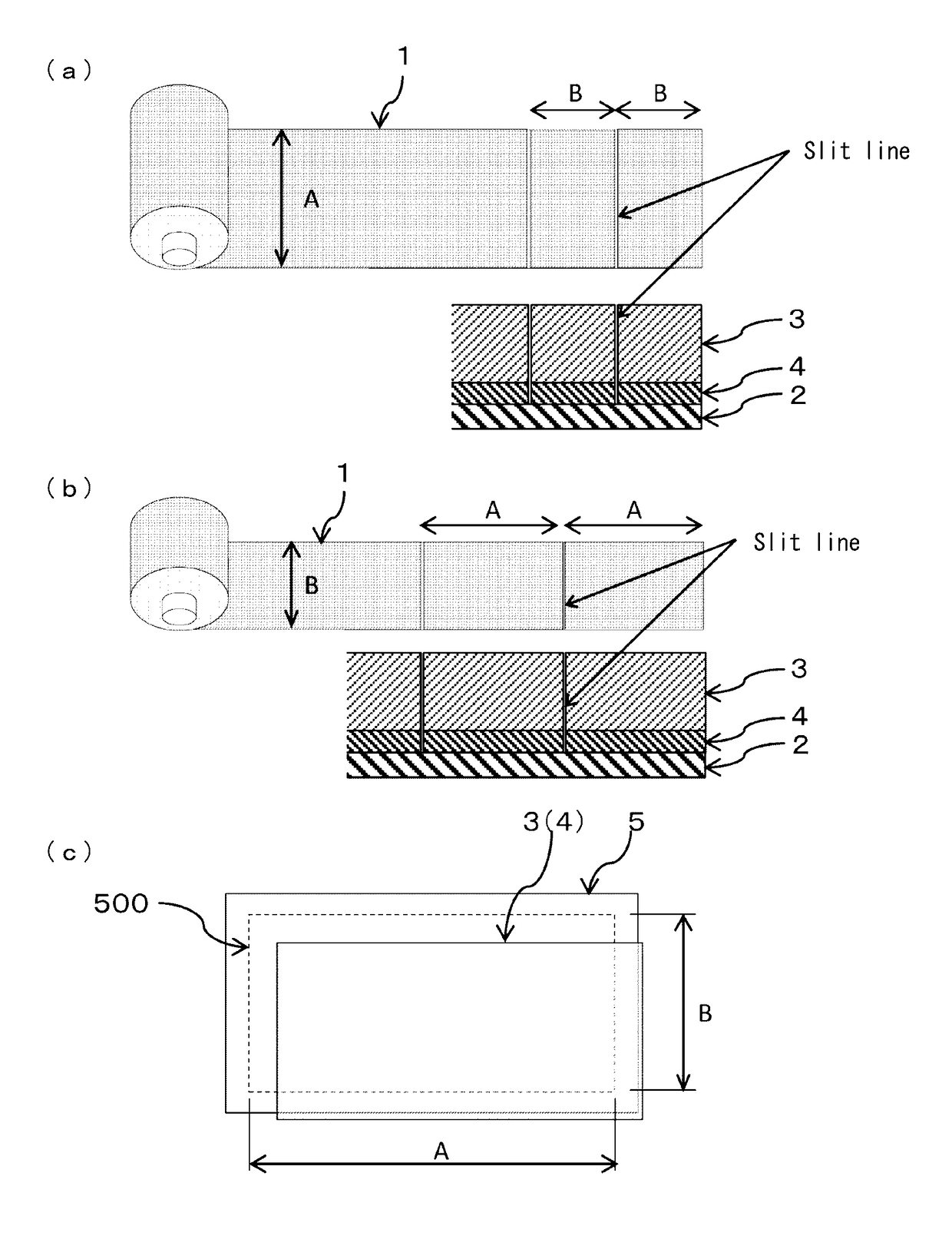
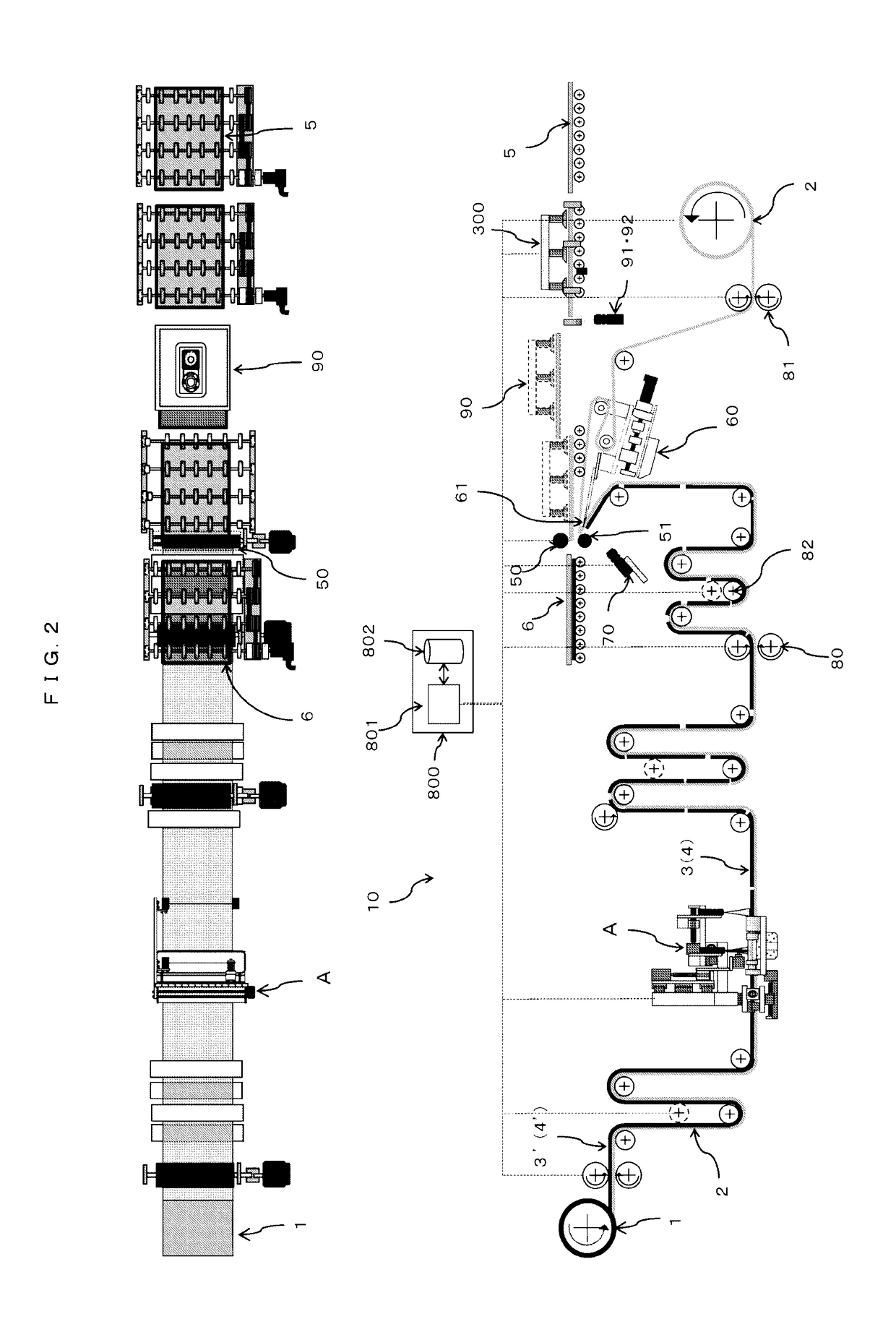
[0061]FIG. 2 illustrates a top view and a side view showing an entire apparatus 10 for manufacturing an optical display device 6 by laminating an optical film sheet 3 and a panel component 5 at a predetermined laminating position 100. The apparatus is provided with lamination rollers 50, 51 configured to open / close in upward / downward direction with respect to feeding direction at a predetermined laminating position 100, and a movable peeling member 60 capable of going in / out of a space 400 formed between the lamination rollers 50, 51 and movable between the space 400 and an operation-start position 200.

[0062]As apparent from FIG. 3, a carrier film 2, in a state where one surface thereof is folded to inside at a tip-end 61 configuring a head portion of the movable peeling member 60 and the carrier film is passed around the movable peeling member 60, supports a leading end 31 of an optical film sheet 3 in...


PUM

PropertyMeasurementUnit
sizeaaaaaaaaaa
sizeaaaaaaaaaa
weightaaaaaaaaaa

Abstract

A method for manufacturing an optical display device comprises: sequentially peeling a plurality of optical film sheets continuously supported via an adhesive layer on one of opposite surfaces of a carrier film, together with the adhesive layer from the carrier film under peeling action of the movable peeling member by winding a long web of the carrier film in a state where the other of opposite surfaces thereof being folded to inside at a tip-end of the movable peeling member having the tip-end and passed around the peeling member; and laminating the plurality of optical film sheets to one of opposite surfaces of respective ones of panel components via the adhesive layer under laminating action of the closed lamination rollers.

Description

CROSS REFERENCE TO RELATED APPLICATION[0001]This application claims the priority of Japanese Patent Application No. 2012-224715, filed on Oct. 10, 2012, and Japanese Patent Application No. 2013-198001, filed on Sep. 25, 2013, in the JPO (Japan Patent Office). Further, this application is the National Phase application of International Application No. PCT / JP2013 / 076470 filed Sep. 30, 2013, which designates the United States and was published in Japanese.TECHNICAL FIELD[0002]The present invention relates to a method and an apparatus for manufacturing an optical display device, the method and the apparatus using lamination rollers configured to open / close in upward / downward direction with respect to feeding direction and a movable peeling member having a tip-end capable of going into / out of a space formed between the lamination rollers. In particular, the present invention relates to a method and an apparatus for manufacturing an optical display device, for sequentially peeling a plura...

Claims


Application Information

Patent Timeline
Patent Type & Authority Patents(United States)
IPC IPC(8): B32B38/10B65H37/00G02F1/1333G02F1/1335B29C63/02G02F1/13
CPCG02F1/1303B29C63/02B32B38/10B65H37/002G02F1/1335G02F1/133308B32B2457/20B65H2701/194G02F2001/133322G02F2001/133325G02F2202/28G02F1/133322G02F1/133325
Inventor YURA, TOMOKAZUTAWADA, AKIRAKOSHIO, SATORUMISHIMA, JUNNAKAZONO, TAKUYA
Owner NITTO DENKO CORP
Why Eureka
Try Eureka