Supercharge Your Innovation With Domain-Expert AI Agents!

Photoconductor, image forming apparatus, and process cartridge

a technology of photoconductor and image forming apparatus, applied in optics, instruments, electrography/magnetography, etc., can solve the problems of affecting the quality of output images, deterioration of photoconductor electric properties, and inability to retain electric stability, and achieve the effect of low transmittance of the undercoat layer

Active Publication Date: 2017-09-19
RICOH KK
View PDF17 Cites 0 Cited by
  • Summary
  • Abstract
  • Description
  • Claims
  • Application Information

AI Technical Summary

Benefits of technology

The solution provides a photoconductor with enhanced stability and reduced background fog, maintaining excellent electric properties and image quality even under varying usage conditions.

Problems solved by technology

As a result, the photoconductor is deteriorated in electric property, and cannot retain electric stability when the photoconductor is used for a long term.
It is known that deterioration in charging property considerably adversely affects quality in output images, and causes serious problems such as deterioration in image quality, background fog (hereinafter may be referred to as background stain, fog, and black spots), poor uniformity of images during continuous outputs.

Method used


Image

  • Photoconductor, image forming apparatus, and process cartridge
  • Photoconductor, image forming apparatus, and process cartridge
  • Photoconductor, image forming apparatus, and process cartridge

Examples


first embodiment

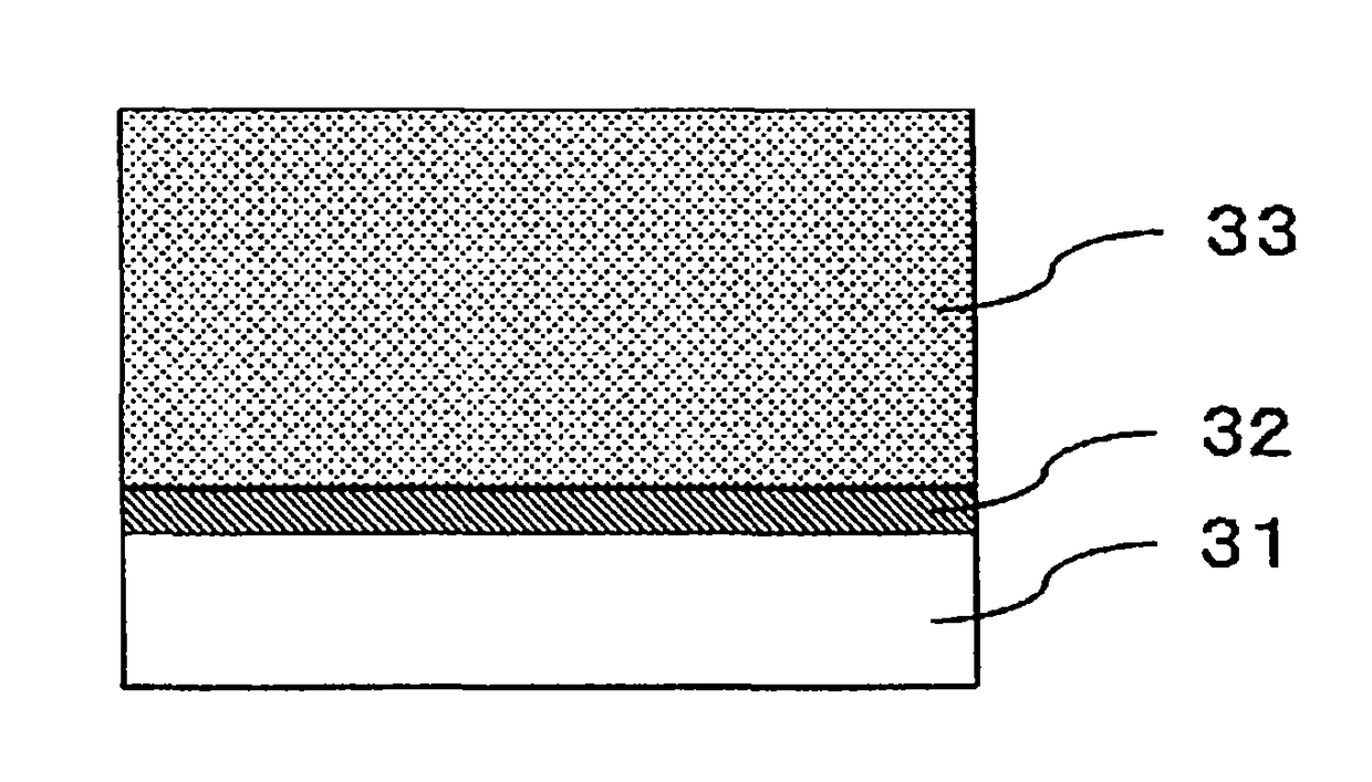
[0172]A layer configuration of the photoconductor according to a first embodiment will be described with reference to FIG. 1.

[0173]FIG. 1 is a structure containing a single-layer photoconductive layer, and is a view illustrating a layer configuration of the photoconductor where an undercoat layer 32 is disposed on a conductive support 31, and a single-layer photoconductive layer 33 is disposed on the undercoat layer 32.

second embodiment

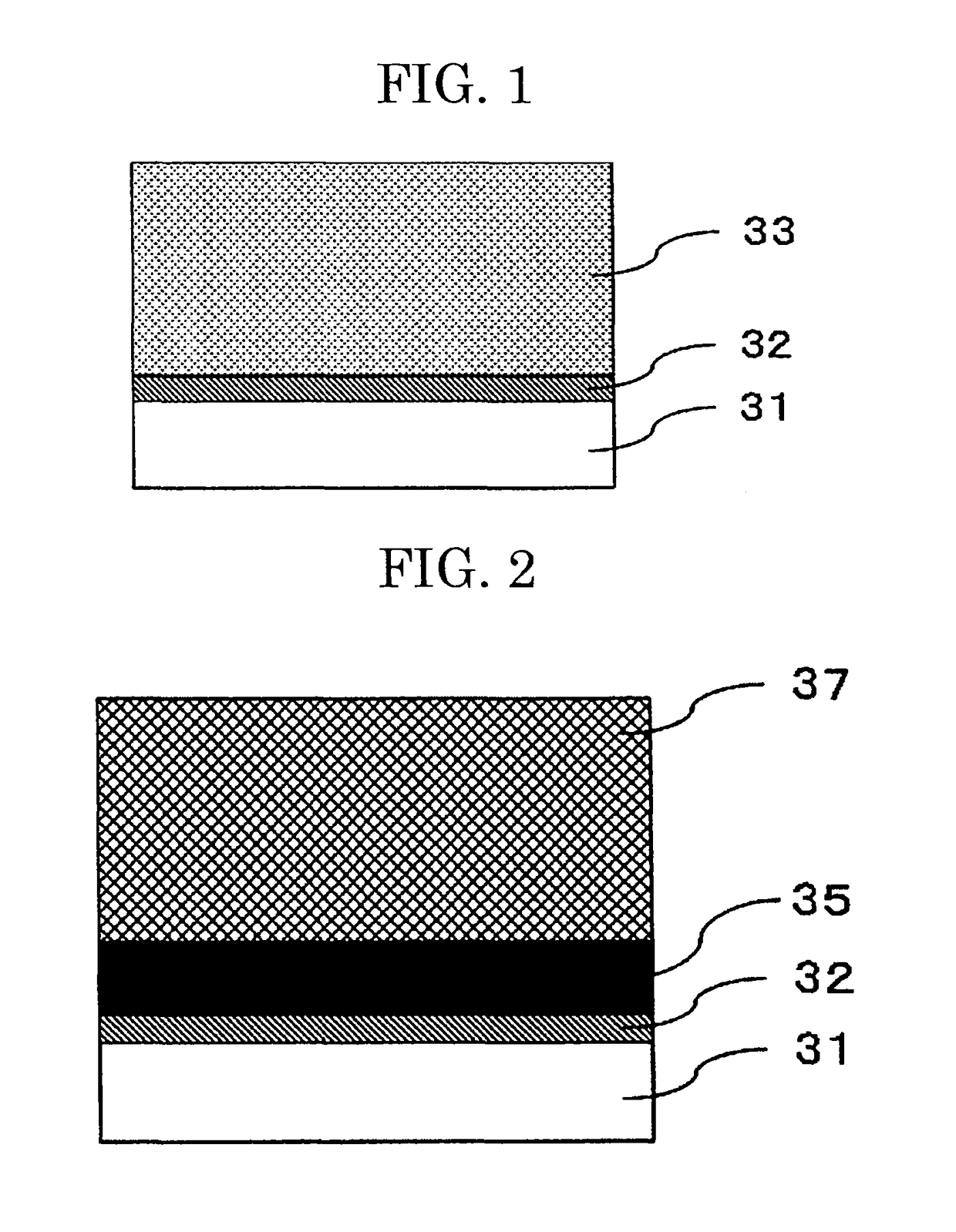
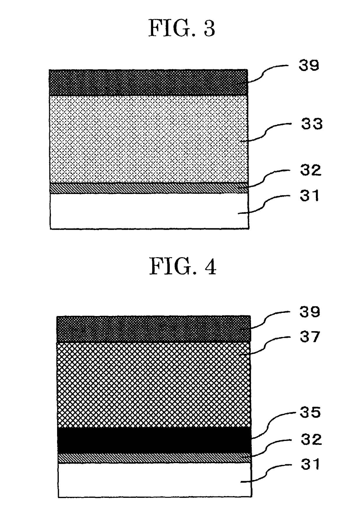
[0174]A layer configuration of the photoconductor according to a second embodiment will be described with reference to FIG. 2.

[0175]FIG. 2 is a structure containing a laminated photoconductive layer, and is a view illustrating a layer configuration of the photoconductor where an undercoat layer 32 is disposed on a conductive support 31, a charge generating layer 35 is disposed on the undercoat layer 32, and a charge transport layer 37 is disposed on the charge generating layer 35. Here, the charge generating layer 35 and the charge transport layer 37 correspond to the photoconductive layer.

third embodiment

[0176]A layer configuration of the photoconductor according to a third embodiment will be described with reference to FIG. 3.

[0177]FIG. 3 is a structure containing a single-layer photoconductive layer, and is a view illustrating a layer configuration of the photoconductor where an undercoat layer 32 is disposed on the conductive support 31, the photoconductive layer 33 is disposed on the undercoat layer 32, and a protective layer 39 is disposed on the photoconductive layer 33.


PUM

PropertyMeasurementUnit
thicknessaaaaaaaaaa
thicknessaaaaaaaaaa
transmittanceaaaaaaaaaa

Abstract

A photoconductor including: a conductive support; an undercoat layer; and a photoconductive layer, the undercoat layer being disposed over the conductive support, the photoconductive layer being disposed over the undercoat layer, wherein the undercoat layer includes zinc oxide particles, wherein when a film thickness of the undercoat layer is 20 μm, the undercoat layer has transmittance of 50% or more to light having a wavelength in a range of 500 nm or more but 800 nm or less, wherein a lowest transmittance of light is 85% or less in the range, and wherein when an electric field of 5 V / μm is applied to the undercoat layer, volume resistivity of the undercoat layer is 1.0×10⁷ Ω·cm or more but 5.0×10⁸ Ω·cm or less at an environment of 23° C. and 55% RH.

Description

CROSS-REFERENCE TO RELATED APPLICATIONS[0001]The present application claims priority under 35 U.S.C. §119 to Japanese Patent Application No. 2015-098281, filed May 13, 2015. The contents of which are incorporated herein by reference in their entirety.BACKGROUND OF THE INVENTION[0002]Field of the Invention[0003]The present disclosure relates to photoconductors, image forming apparatuses including the photoconductors, and process cartridges including the photoconductors.[0004]Description of the Related Art[0005]In an image forming method using an image forming apparatus, an image is formed by subjecting a photoconductor to, for example, a charging step, an exposure step, a developing step, and a transfer step. Recently, an organic photoconductor containing an organic material is widely used as a photoconductor because of advantages such as flexibility, thermal stability, and film-forming property.[0006]Recently, there is a need for photoconductors to have greater degrees of durability...

Claims


Application Information

Patent Timeline
Patent Type & Authority Patents(United States)
IPC IPC(8): G03G5/147G03G5/14G03G21/18
CPCG03G5/144G03G5/142G03G5/1476G03G5/14765G03G21/18
Inventor ISHIDA, TOSHIHIROKURIMOTO, EIJISUZUKI, TETSUROASANO, TOMOHARUNII, DAISUKE
Owner RICOH KK
Features
  • R&D
  • Intellectual Property
  • Life Sciences
  • Materials
  • Tech Scout
  • Unparalleled Data Quality
  • Higher Quality Content
  • 60% Fewer Hallucinations
Learn More