Eureka AIR delivers breakthrough ideas for toughest innovation challenges, trusted by R&D personnel around the world.

Reduced silicon-oxide-nitride-oxide-silicon (SONOS) flash memory program disturb

Inactive Publication Date: 2017-09-26
QUALCOMM INC
View PDF9 Cites 1 Cited by
  • Summary
  • Abstract
  • Description
  • Claims
  • Application Information

AI Technical Summary

Benefits of technology

The patent text describes a method for balancing voltage stress in a silicon-oxide-nitride-oxide-silicon (SONOS) flash memory array. The method involves selecting a particular cell for programming and determining the voltage stress associated with the programmed cells and their unselected neighbors. The unselected cells are coupled to the same word line or bit line as the programmed cell. The method then balances the voltage stress to enable the SONOS flash memory array to be programmed according to a sub-page program mode. The technical effect of this patent is to improve the reliability and performance of SONOS flash memory arrays by balancing voltage stress and reducing programmed cell damage.

Problems solved by technology

As a result, the SONOS transistors in the unselected SONOS memory cells may experience program disturb.
A voltage difference between the gate and drain of a SONOS transistor in an unselected SONOS memory cell may result in voltage stress across the SONOS transistor.
The voltage stress may cause the unselected SONOS memory cell to experience program disturb.
For example, the voltage stress may cause the unselected SONOS memory cell to be inadvertently programmed.

Method used


Image

  • Reduced silicon-oxide-nitride-oxide-silicon (SONOS) flash memory program disturb
  • Reduced silicon-oxide-nitride-oxide-silicon (SONOS) flash memory program disturb
  • Reduced silicon-oxide-nitride-oxide-silicon (SONOS) flash memory program disturb

Examples


Embodiment Construction

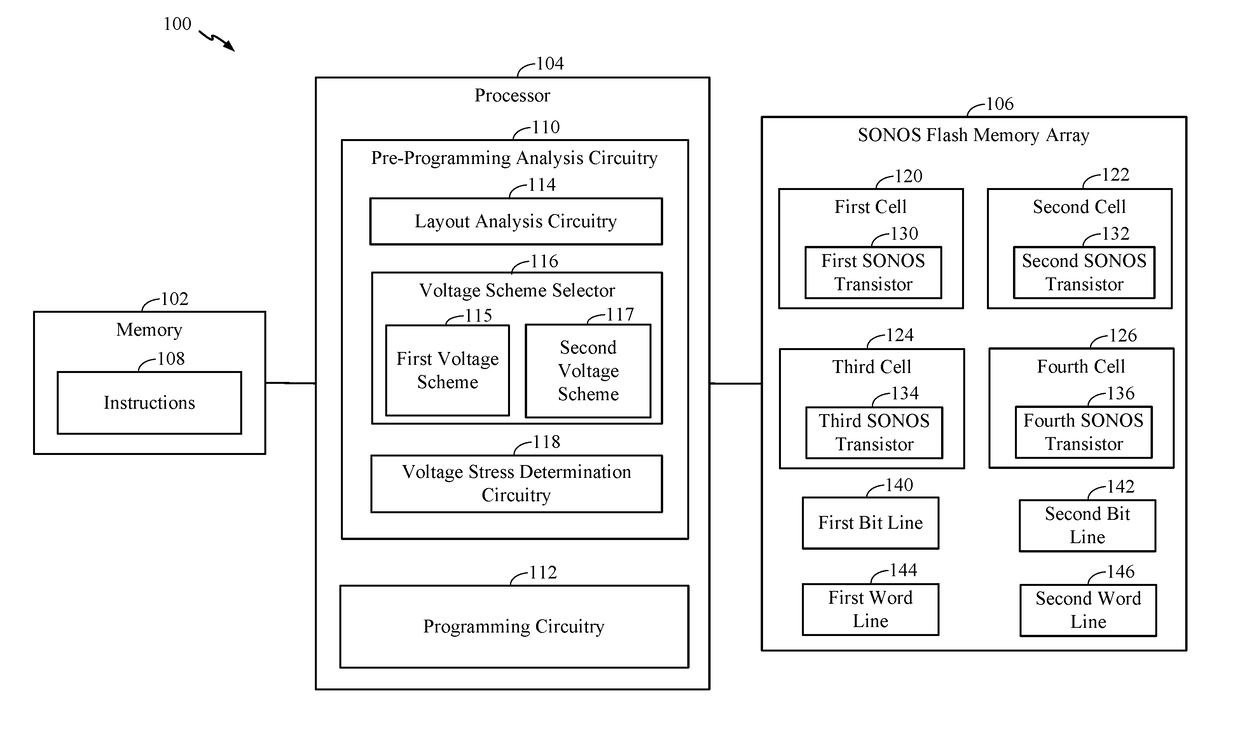
[0013]Referring to FIG. 1, a system 100 that is operable to balance voltage stress at a silicon-oxide-nitride-silicon (SONOS) flash memory is shown. The system 100 includes a memory 102, a processor 104, and a SONOS flash memory array 106. According to one implementation, the SONOS flash memory array 106 may be a SONOS embedded-flash (eFlash) memory array. The memory 102 is coupled to the processor 104, and the processor 104 is coupled to the SONOS flash memory array 106.

[0014]The memory 102 includes instructions 108 that are executable by one or more components of the processor 104 to perform the techniques described herein. According to one implementation, the memory 102 includes a non-transitory computer-readable medium. The processor 104 includes pre-programming analysis circuitry 110 and programming circuitry 112. The pre-programming analysis circuitry 110 includes layout analysis circuitry 114, a voltage scheme selector 116, and voltage stress determination circuitry 118.

[0015...


PUM


Abstract

A method and apparatus for balancing voltage stress at a silicon-oxide-nitride-oxide-silicon (SONOS) flash memory array is disclosed. A particular cell of the SONOS flash memory array is selected for programming. A first voltage stress associated with a first SONOS transistor is determined if the particular cell is programmed. The first SONOS transistor is included in a first unselected cell of the SONOS flash memory array. A second voltage stress associated with a second SONOS transistor is determined if the particular cell is programmed. The first voltage stress and the second voltage stress are balanced prior to programming the particular cell.

Description

I. FIELD[0001]The present disclosure is generally related to an innovative methodology to reduce silicon-oxide-nitride-oxide-silicon (SONOS) flash memory program disturb.II. DESCRIPTION OF RELATED ART[0002]Advances in technology have resulted in smaller and more powerful computing devices. For example, there currently exist a variety of portable personal computing devices, including wireless computing devices, such as portable wireless telephones and smart watches, and paging devices that are small, lightweight, and easily carried by users. More specifically, portable wireless telephones, such as cellular telephones and Internet protocol (IP) telephones, can communicate voice and data packets over wireless networks. Further, many such wireless telephones include other types of devices that are incorporated therein. For example, a wireless telephone can also include a digital still camera, a digital video camera, a digital recorder, and an audio file player. Also, such wireless telep...

Claims


Application Information

Patent Timeline
IPC IPC(8): G11C16/10G11C16/34
CPCG11C16/3427G11C16/10G11C16/3422G11C16/0466G11C16/3418
Inventor WANG, ZHONGZECHEN, GUOQINGHOAYUN, PAUL
Owner QUALCOMM INC
Why Eureka
Eureka Blog
Learn More