Semiconductor memory device for performing refresh operation and operating method therof

a memory device and memory technology, applied in the field can solve the problems of reducing the integration of semiconductor memory devices, affecting the performance of memory devices, and affecting the operation of memory devices

Active Publication Date: 2017-10-10
SK HYNIX INC
View PDF5 Cites 62 Cited by
  • Summary
  • Abstract
  • Description
  • Claims
  • Application Information

AI Technical Summary

Problems solved by technology

However, the electric charge stored in the cell capacitor changes due to a voltage difference from a surrounding circuit.
As substantial change in the electric charge of the cell capacitor due to a leakage current, may result in data stored in the cell capacitor to be changed or lost.
However, as the size of a memory bank becomes smaller, the intervals between memory cells and between neighboring word lines also become smaller.
Recently, the interval between word lines has become so small that a coupling effect between adjacent word lines may occur causing neighboring memory cells to lose data stored therein.
However, too many refresh operations may degrade the overall operation efficiency of the semiconductor memory device.

Method used


Image

  • Semiconductor memory device for performing refresh operation and operating method therof
  • Semiconductor memory device for performing refresh operation and operating method therof
  • Semiconductor memory device for performing refresh operation and operating method therof

Examples


Embodiment Construction

[0030]Various embodiments will be described below in more detail with reference to the accompanying drawings. The present invention may, however, be embodied in different forms and should not be construed as being limited to the embodiments set forth herein. Rather, these embodiments are provided so that this disclosure will be thorough and complete, and will fully convey the present invention to those skilled in the art. Throughout the disclosure, like reference numerals refer to like parts throughout the various figures and embodiments of the present invention.

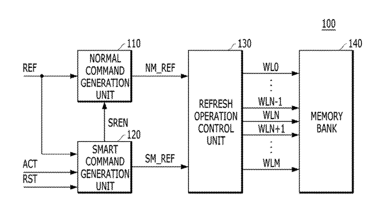
[0031]Referring now to FIG. 1 a semiconductor memory device is provided, according to an embodiment of the present invention.

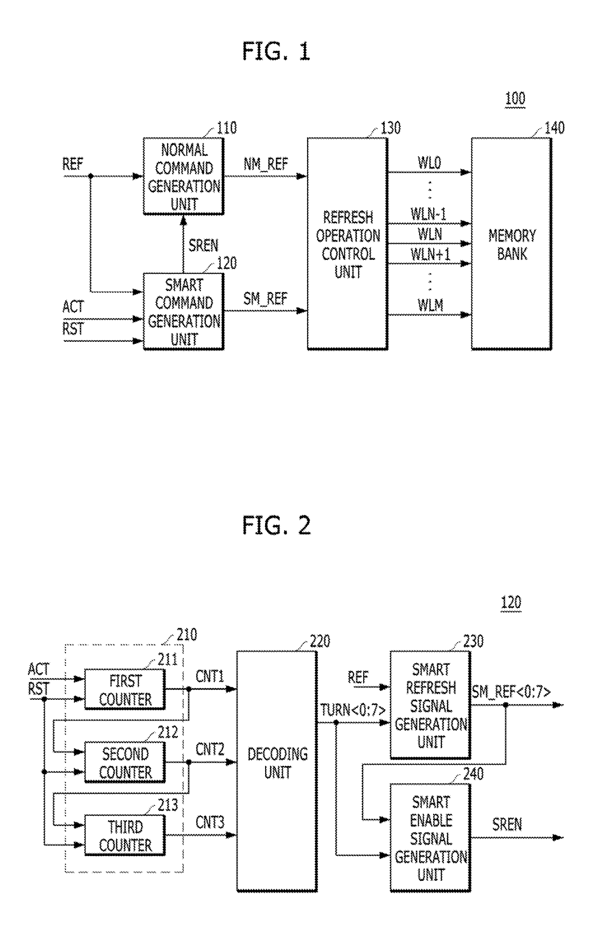
[0032]According to the embodiment of FIG. 1, the semiconductor memory device 100 may include a normal command generation unit 110, a smart command generation unit 120, a refresh operation control unit 130, and a memory bank 140.

[0033]The normal command generation unit 110 may generate a normal refresh ...


PUM


Abstract

A semiconductor memory device may include: a memory bank comprising a plurality of word lines; a smart command generation unit suitable for generating a smart refresh command, which is enabled at a random cycle, in response to an active command; and a refresh operation control unit suitable for performing a refresh operation to at least one of adjacent word lines of a target word line among the plurality of word lines in response to the smart refresh command.

Description

CROSS-REFERENCE TO RELATED APPLICATIONS[0001]The present application claims priority of Korean Patent Application No. 10-2015-0188624, filed on Dec. 29, 2015, which is incorporated herein by reference in its entirety.BACKGROUND[0002]1. Field[0003]Exemplary embodiments of the present invention relate to a semiconductor design technology and, more particularly, to a semiconductor memory device which performs a refresh operation.[0004]2. Description of the Related Art[0005]A semiconductor memory device includes a plurality of memory banks for storing data, and each of the memory banks includes tens of millions of memory cells. Each of the memory cells includes a cell capacitor and a cell transistor, and the semiconductor memory device stores data through an operation of charging or discharging the cell capacitor. The electric charge stored in the cell capacitor must be ideally constant in the absence of any interruption. However, the electric charge stored in the cell capacitor changes...

Claims


Application Information

Patent Timeline
Patent Type & Authority Patents(United States)
IPC IPC(8): G11C7/00G11C11/408G11C11/406
CPCG11C11/40615G11C11/4085G11C11/406G11C11/40611
Inventor LEE, SUNG-YUBLEE, GEUN-ILCHA, JAE-HOON
Owner SK HYNIX INC
Why Eureka
Try Eureka