
Processes for shaping nanomaterials

a nanomaterial and processing technology, applied in the field of nanomaterials, can solve the problems of limited treatment of a single nanowire, limited functionality of unpatterned graphene, and inability to perform complex shape changes

Active Publication Date: 2018-01-30
PURDUE RES FOUND INC
View PDF2 Cites 0 Cited by
  • Summary
  • Abstract
  • Description
  • Claims
  • Application Information

AI Technical Summary

Benefits of technology

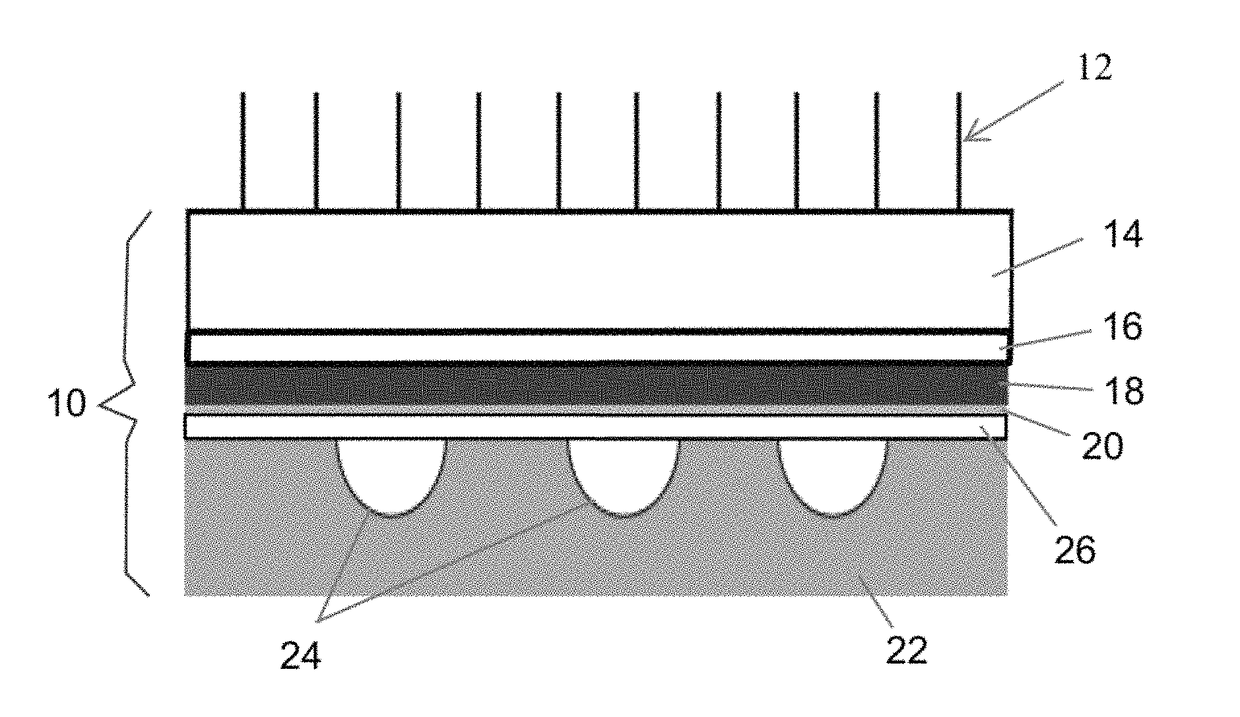
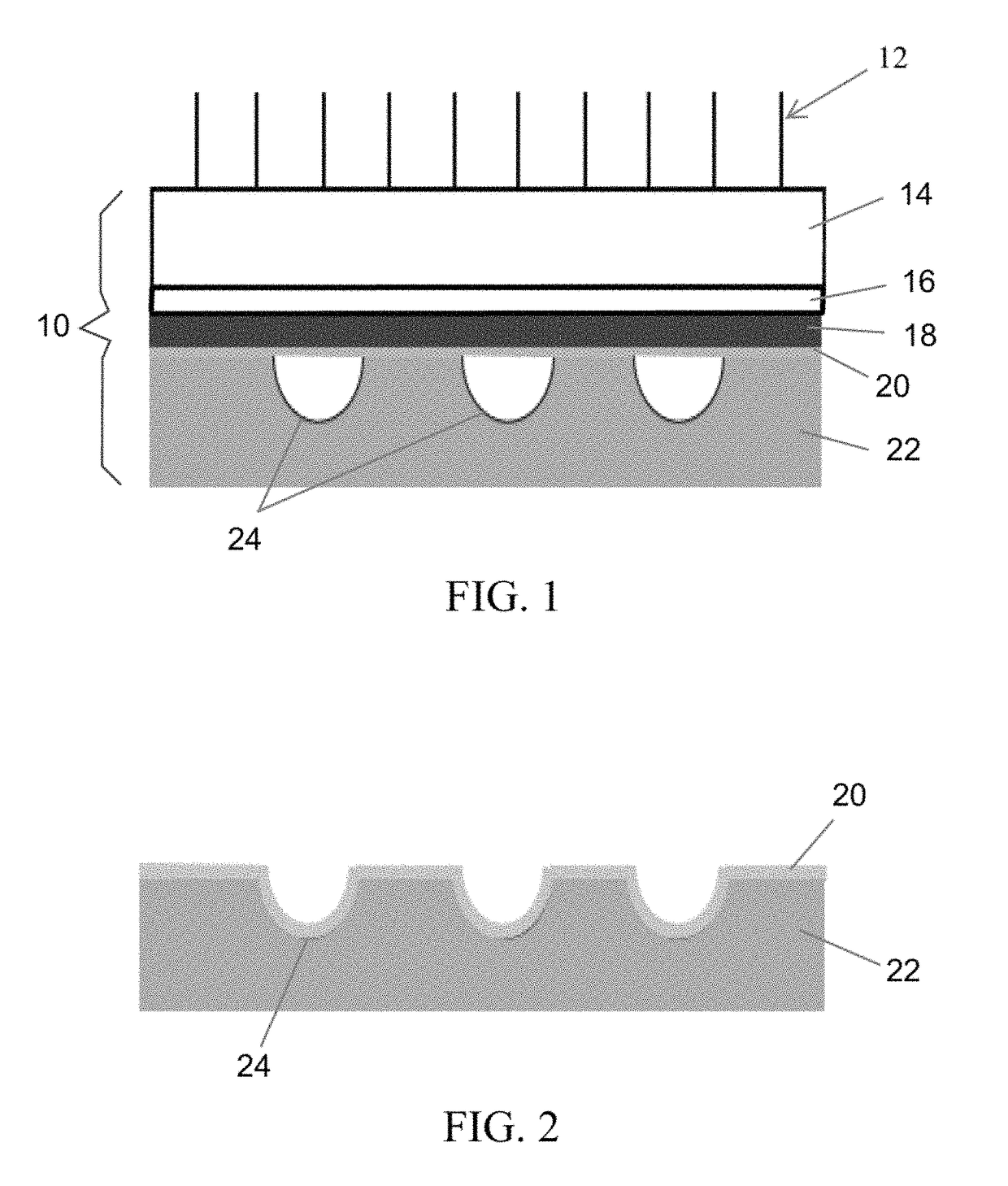
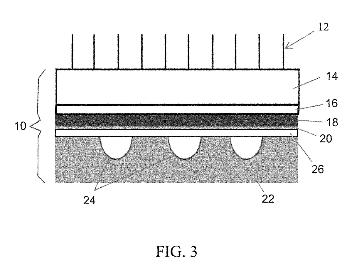
[0008]According to one aspect of the invention, a process is provided that includes providing a substrate comprising a three-dimensional surface feature thereon formed, locating a nanomaterial on the substrate and over the surface feature, directing a laser beam toward the nanomaterial such that the nanomaterial experiences laser shock pressure sufficient to deform the nanomaterial to conform at least partially to the shape of the surface feature and adhere to the surface feature either directly or via an intermediate layer therebetween, and controlling the deformation of the nanomaterial to tunably modify a material property of the nanomaterial.
[0009]According to another aspect of the invention, a process is provided that includes providing a substrate comprising a three-dimensional surface feature thereon, locating a one-dimensional nanomaterial on the substrate and over the surface feature, and directing a laser beam toward the nanomaterial such that the nanomaterial experiences laser shock pressure sufficient to deform the nanomaterial to conform at least partially to the shape of the surface feature and adhere to the surface feature either directly or via an intermediate layer therebetween without causing fracture in the nanomaterial.

Problems solved by technology

However, current NW processing techniques cannot perform complicated shape changes and are limited to treating a single nanowire at a time.
However, due to having zero band gaps, unpatterned graphene has limited functionality.
One approach has been developed that produces graphene nanoribbons and dots to increase band gaps, but reliability, scalability, and quality remain issues for graphene patterning.

Method used


Image

  • Processes for shaping nanomaterials
  • Processes for shaping nanomaterials
  • Processes for shaping nanomaterials

Examples


Embodiment Construction

[0025]The present invention provides processes for shaping 1D and 2D nanomaterials using laser or other high speed intensive optical source processing systems, referred to herein as laser shock strain engineering (LSSE) processes. In particular, laser shock pressure can be employed to perform various forming approaches, including but not limited to conformal shaping, uniform bending, cutting, and lateral compression, preferably without unintentionally fracturing or cracking the nanomaterial. Such capability can be used to create nanomaterials with tunable shapes, allowing for the accommodation of various structural requirements, including flexible electronics. Such a capability can also be used to tunably change various properties of nanomaterials, for example, electrical, chemical, and optical properties, which may provide opportunities for developing miniature devices, for example, for use in electronics. According to a nonlimiting aspect of the invention, local strains may be ind...


PUM

PropertyMeasurementUnit
widthaaaaaaaaaa
widthaaaaaaaaaa
temperatureaaaaaaaaaa

Abstract

Processes for shaping one- and two-dimensional nanomaterials, and thereby inducing local strains therein preferably to control one or more of their material properties. The processes include providing a substrate comprising a three-dimensional surface feature thereon, locating a nanomaterial on the substrate and over the surface feature, and directing a laser beam toward the nanomaterial such that the nanomaterial experiences laser shock pressure sufficient to deform the nanomaterial to conform at least partially to the shape of the surface feature and adhere to the surface feature either directly or via an intermediate layer therebetween.

Description

CROSS REFERENCE TO RELATED APPLICATIONS[0001]This application claims the benefit of U.S. Provisional Application Nos. 62 / 302,503 and 62 / 302,369, both filed Mar. 2, 2016, the contents of which are incorporated herein by reference.BACKGROUND OF THE INVENTION[0002]The present invention generally relates to nanomaterials. The invention particularly relates to one- and two-dimensional nanomaterials and to methods for their processing.[0003]Nanomaterials are the subject of significant research across a broad spectrum of industries. As used herein, the term “nanomaterials” refers to materials with all dimensions being nanoscale (as nonlimiting examples, quantum dots, nanoparticles, dendrimers, nanocapsules, Fullerenes, nanoclusters, and nanodispersions) (zero-dimensional (0D) nanomaterials), materials with two dimensions being nanoscale and the third dimension being greater than nanoscale (as nonlimiting examples, nanofibers, nanotubes, nanowires, and nanorods) (one-dimensional (1D) nanoma...

Claims


Application Information

Patent Timeline
Patent Type & Authority Patents(United States)
IPC IPC(8): B82Y30/00B82B3/00H01L21/268H01L21/02
CPCH01L21/02664B82B3/008H01L21/02527H01L21/268H01L21/02568H01L21/02603H01L21/02653H01L21/02532B81C1/00634H01L21/0243
Inventor CHENG, GARY J.
Owner PURDUE RES FOUND INC
Learn More