Display panel with touch detection function

a display panel and function technology, applied in the field of display panel with touch detection function, can solve the problems of reducing the detection accuracy of the touch position is remarkably reduced, and the pixel aperture ratio is reduced, so as to achieve the effect of reducing the pixel aperture ratio, and remarkably reducing the display quality

Active Publication Date: 2018-03-06
PANASONIC INTELLECTUAL PROPERTY CORP OF AMERICA
View PDF34 Cites 12 Cited by
  • Summary
  • Abstract
  • Description
  • Claims
  • Application Information

AI Technical Summary

Benefits of technology

[0006]However, in the technology disclosed in the above-mentioned publication, the following two problems mainly arise. The first problem resides in that a pixel aperture ratio is reduced. FIG. 29 is a plan view of a display panel disclosed in the above-mentioned publication. As illustrated in FIG. 29, when a sensor electrode line 706 is formed adjacent to a source line 704, the sensor electrode line 706 is arranged in a pixel aperture region. In this case, the pixel aperture ratio is reduced, and the display quality is remarkably reduced. The second problem resides in that the detection accuracy of the touch position is reduced. When the sensor electrode line 706 is formed close to a gate line 702, a parasitic capacitance formed between the sensor electrode line 706 and the gate line 702 is increased. In this case, due to the influence of the above-mentioned parasitic capacitance, the detection accuracy of the touch position is remarkably reduced.
[0007]The present application has been made in view of the above-mentioned problems, and has an object to provide a display panel with touch detection function, which is high in pixel aperture ratio and excellent in detection accuracy of the touch position.

Problems solved by technology

However, in the technology disclosed in the above-mentioned publication, the following two problems mainly arise.
The first problem resides in that a pixel aperture ratio is reduced. FIG. 29 is a plan view of a display panel disclosed in the above-mentioned publication.
The second problem resides in that the detection accuracy of the touch position is reduced.
In this case, due to the influence of the above-mentioned parasitic capacitance, the detection accuracy of the touch position is remarkably reduced.

Method used


Image

  • Display panel with touch detection function
  • Display panel with touch detection function
  • Display panel with touch detection function

Examples


first embodiment

[0060]FIG. 4 is a sectional view taken along the line A-A′ of FIG. 2 in the display panel 10 of the first embodiment. The display panel 10 includes a TFT substrate 200, a color filter (CF) substrate 300, and a liquid crystal layer 400 sandwiched between both the substrates.

[0061]In the TFT substrate 200, the plurality of gate signal lines 13 (not shown) are formed on a glass substrate 201, a first insulating film 202 is formed so as to cover the plurality of gate signal lines 13, the plurality of data signal lines 11 are formed on the first insulating film 202, a second insulating film 203 is formed so as to cover the plurality of data signal lines 11, and a third insulating film 204 is formed on the second insulating film 203. The third insulating film 204 is made of, for example, a photosensitive organic material containing acrylic as a main component. The plurality of common electrodes 17 (sensor electrodes) are formed on the third insulating film 204, a fourth insulating film 20...

second embodiment

[0064]FIG. 5 is a sectional view taken along the line A-A′ of FIG. 2 in a display panel 10 of the second embodiment.

[0065]In the TFT substrate 200, the plurality of gate signal lines 13 (not shown) are formed on the glass substrate 201, the first insulating film 202 is formed so as to cover the plurality of gate signal lines 13, the plurality of data signal lines 11 are formed on the first insulating film 202, the second insulating film 203 is formed so as to cover the plurality of data signal lines 11, and the third insulating film 204 (organic insulating film) is formed on the second insulating film 203. The plurality of sensor electrode lines 12 are formed on the third insulating film 204, the fourth insulating film 205 is formed so as to cover the plurality of sensor electrode lines 12, and the through hole 18 is formed through a part of the fourth insulating film 205. The sensor electrode line 12 is formed at a position at which the sensor electrode line 12 overlaps with the da...

third embodiment

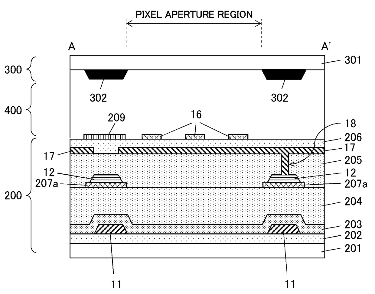
[0068]FIG. 6 is a sectional view taken along the line A-A′ of FIG. 2 in a display panel 10 of the third embodiment. The display panel 10 of the third embodiment is formed as follows. In the display panel 10 of the second embodiment, a plurality of adhesion layers 207a are formed on the third insulating film 204, and the sensor electrode lines 12 are formed on the respective adhesion layers 207a. The adhesion layer 207a and the sensor electrode line 12 are formed at a position at which the adhesion layer 207a and the sensor electrode line 12 overlap with the data signal line 11 in plan view. The adhesion layer 207a is made of, for example, indium tin oxide (ITO), which is a transparent conductive material.

[0069]With the above-mentioned configuration, the above-mentioned effects in the display panel 10 of the second embodiment can be obtained, and it is possible to prevent film removal of the sensor electrode line 12 from the third insulating film 204.


PUM


Abstract

Provided is a display panel including: a plurality of pixel electrodes divided into a plurality of groups; and a plurality of common electrodes arranged at a ratio of one to a plurality of pixel electrodes included in one of the plurality of groups. Each of a plurality of sensor electrode lines overlaps with corresponding one of a plurality of data signal lines in plan view. The plurality of sensor electrode lines and each of the plurality of common electrodes overlap each other in plan view. The each of the plurality of common electrodes is electrically connected to the plurality of sensor electrode lines. At least one insulating film is formed between each of a region between the data signal lines and the sensor electrode lines, a region between the sensor electrode lines and the common electrodes, and a region between the common electrodes and the pixel electrodes.

Description

CROSS REFERENCE TO RELATED APPLICATIONS[0001]The present application claims priority to Provisional application No. 62 / 121,515 filed on Feb. 27, 2015.BACKGROUND[0002]1. Field of the Invention[0003]The present application relates to a display panel with touch detection function.[0004]2. Description of the Related Art[0005]Hitherto, various display devices with touch panels have been proposed. In recent years, in order to reduce the thickness of the entire display device, there has been proposed a so-called in-cell display device with touch detection function, which incorporates a function of a touch panel inside a display panel. The above-mentioned display device is disclosed in, for example, U.S. Pat. No. 8,766,950. Further, in the above-mentioned publication, there is disclosed an in-plane switching (IPS) display panel that is excellent in wide viewing angle characteristics.SUMMARY[0006]However, in the technology disclosed in the above-mentioned publication, the following two probl...

Claims


Application Information

Patent Timeline
Patent Type & Authority Patents(United States)
IPC IPC(8): G06F3/045G06F3/041G06F3/047G06F3/044
CPCG06F3/0416G06F3/044G06F3/047G06F3/0412G06F2203/04112G06F2203/04103G06F2203/04111G02F1/136286G02F1/134309G06F3/041G09G3/3648G06F3/04164G06F3/0443
Inventor AOYAMA, TOSHIYUKIFUKAMI, TETSUOKAJITA, DAISUKETAKAGI, KAZUSHIGE
Owner PANASONIC INTELLECTUAL PROPERTY CORP OF AMERICA
Why Eureka
Try Eureka