Using sense amplifier as a write booster in memory operating with a large dual rail voltage supply differential

a dual-rail voltage supply and memory technology, applied in the direction of information storage, static storage, digital storage, etc., can solve the problems of large write drivers, large circuit layout, and inability to write at the same time, so as to improve the reliability and speed of write operations, and boost write voltages

Active Publication Date: 2018-05-08
SYNOPSYS INC
View PDF12 Cites 0 Cited by
  • Summary
  • Abstract
  • Description
  • Claims
  • Application Information

AI Technical Summary

Benefits of technology

[0005]Accordingly, a method and structure are provided for using a sense amplifier to boost write voltages, thereby improving the reliability and speed of write operations performed in a memory having a differential between an array supply voltage and a periphery supply voltage, or a low periphery supply voltage.
[0006]In a particular embodiment, a memory includes a memory cell that operates in response to an array supply voltage VA, and a pair of bit lines coupled to the memory cell, wherein the bit lines are pre-charged to a periphery supply voltage VDDP prior to accesses to the memory cell, wherein the periphery supply voltage VDDP is less than the array supply voltage VA. The memory further includes a sense amplifier that operates in response to the periphery supply voltage during accesses to the memory cell, and a first pair of transistors that couple the sense amplifier to the bit lines during write accesses to the memory cell, such that the sense amplifier pulls one of the bit lines toward the periphery supply voltage VDDP, and pulls the other one of the bit lines toward the VSS (ground) supply voltage. By coupling the sense amplifier to the bit lines during write accesses, the drive of write data voltages onto the bit lines is improved, thereby improving the reliability and speed of the write accesses.

Problems solved by technology

However, writing into a memory cell in a memory system with a large dual rail voltage supply differential (i.e, a large difference between the periphery supply voltage and the memory array supply voltage) or a very low periphery supply voltage is a challenge, and it is possible that write operations will fail, because the memory periphery circuitry (which operates in response to the relatively low periphery supply voltage) is not able to sufficiently drive the bit line voltages to change the state of a data value stored in the memory cell.
Even if write operations are successful, the large differential between the array supply voltage and the periphery supply voltage results in a relatively slow write speed, because the relatively weak drive associated with the memory periphery circuitry will take a relatively long time to change the state of a data value stored in the memory cell.
However, larger write drivers would undesirably require a larger circuit layout and higher power consumption.

Method used


Image

  • Using sense amplifier as a write booster in memory operating with a large dual rail voltage supply differential
  • Using sense amplifier as a write booster in memory operating with a large dual rail voltage supply differential
  • Using sense amplifier as a write booster in memory operating with a large dual rail voltage supply differential

Examples


Embodiment Construction

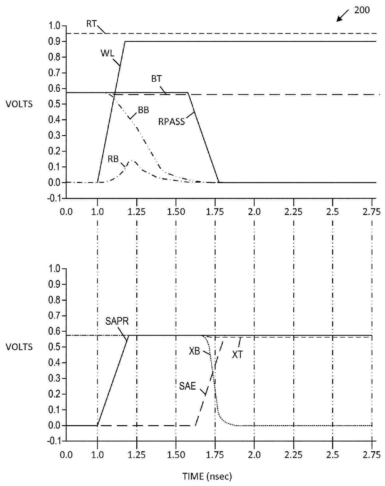
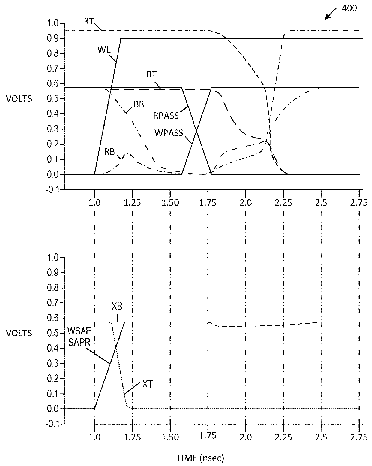
[0014]In general, the present invention provides a method and circuitry for coupling a sense amplifier to bit lines during a write operation, thereby boosting a write voltage developed on the bit lines during the write operation. Boosting the write voltage in this manner advantageously ensures reliable write operations, while adding minimal circuitry to a conventional memory design. Boosting the write voltage in this manner also results in write operations being completed in a relatively fast manner, thereby enabling a fast operating frequency of the memory.

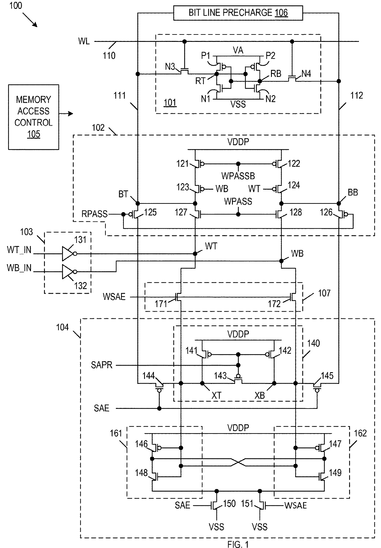
[0015]FIG. 1 is a circuit diagram of a portion of an embedded memory 100, which includes static random access memory (SRAM) cell 101, read / write pass gate circuitry 102, local write driver circuitry 103, sense amplifier circuitry 104, memory access control circuitry 105, bit line pre-charge circuitry 106 and write sense amplifier coupling circuitry 107. In one embodiment, the illustrated elements of embedded memory 100 are fabric...


PUM


Abstract

A memory includes a memory cell that operates in response to an array supply voltage, and a corresponding pair of bit lines that are pre-charged to a periphery supply voltage prior to each access of the memory cell. A sense amplifier coupled to the bit lines operates in response to the periphery supply voltage. The periphery supply voltage is less than the array supply voltage to enable power savings within the memory. A first pair of transistors is configured to couple the sense amplifier to the bit lines during write accesses to the memory cell, thereby boosting the write voltages applied to the bit lines during a write operation. That is, the first pair of transistors is configured such that the sense amplifier pulls one of the bit lines toward the periphery supply voltage (and the other one of the bit lines toward the ground supply voltage) during write accesses.

Description

FIELD OF THE INVENTION[0001]The present invention relates to memories that operate with a large dual rail voltage supply differential. More specifically, the present invention relates to the use of a sense amplifier to boost write operations in a memory having a large differential between a memory array voltage and a peripheral device voltage, or in a memory where the periphery device voltage is very low.RELATED ART[0002]The Internet of Things (IoT) is accelerating rapidly, bringing with it a wealth of opportunities. In the context of embedded memories, such as embedded static random access memories (SRAMs), it is desirable for the memory periphery circuitry to operate at a very low voltage (to minimize power consumption) while the memory array is required to operate at a significantly higher (minimum) voltage. For example, memory periphery circuitry (e.g., write driver circuitry, sense amplifier circuitry, and pass transistors that couple the write driver circuitry and sense amplif...

Claims


Application Information

Patent Timeline
Patent Type & Authority Patents(United States)
IPC IPC(8): G11C7/06G11C11/419G11C11/413G11C7/08G11C7/18
CPCG11C11/419G11C11/413G11C7/18
Inventor SONKAR, DHARMESH KUMARBEHERA, NIRANJAN
Owner SYNOPSYS INC
Why Eureka
Try Eureka