Direct current sum bandgap voltage comparator

a voltage comparator and direct current technology, applied in the field of integrated circuits, can solve the problems of large area on a semiconductor chip, large number of devices needed for implementation, and typical bandgap reference circuits are also fairly sensitive to noise within the circui

Inactive Publication Date: 2007-11-13
STMICROELECTRONICS SRL
View PDF27 Cites 23 Cited by
  • Summary
  • Abstract
  • Description
  • Claims
  • Application Information

AI Technical Summary

Problems solved by technology

One drawback with a typical bandgap reference circuit is that a large number of devices are needed for implementation.
As a result, a large amount of area on a semiconductor chip is required.
In addition to the area problem, typical bandgap reference circuits also are fairly sensitive to noise within the circuit.
For example, active memory circuits are usually noisy and known bandgap circuits used with active memories circuits are usually sensitive to the noise generated.

Method used


Image

  • Direct current sum bandgap voltage comparator
  • Direct current sum bandgap voltage comparator
  • Direct current sum bandgap voltage comparator

Examples


Embodiment Construction

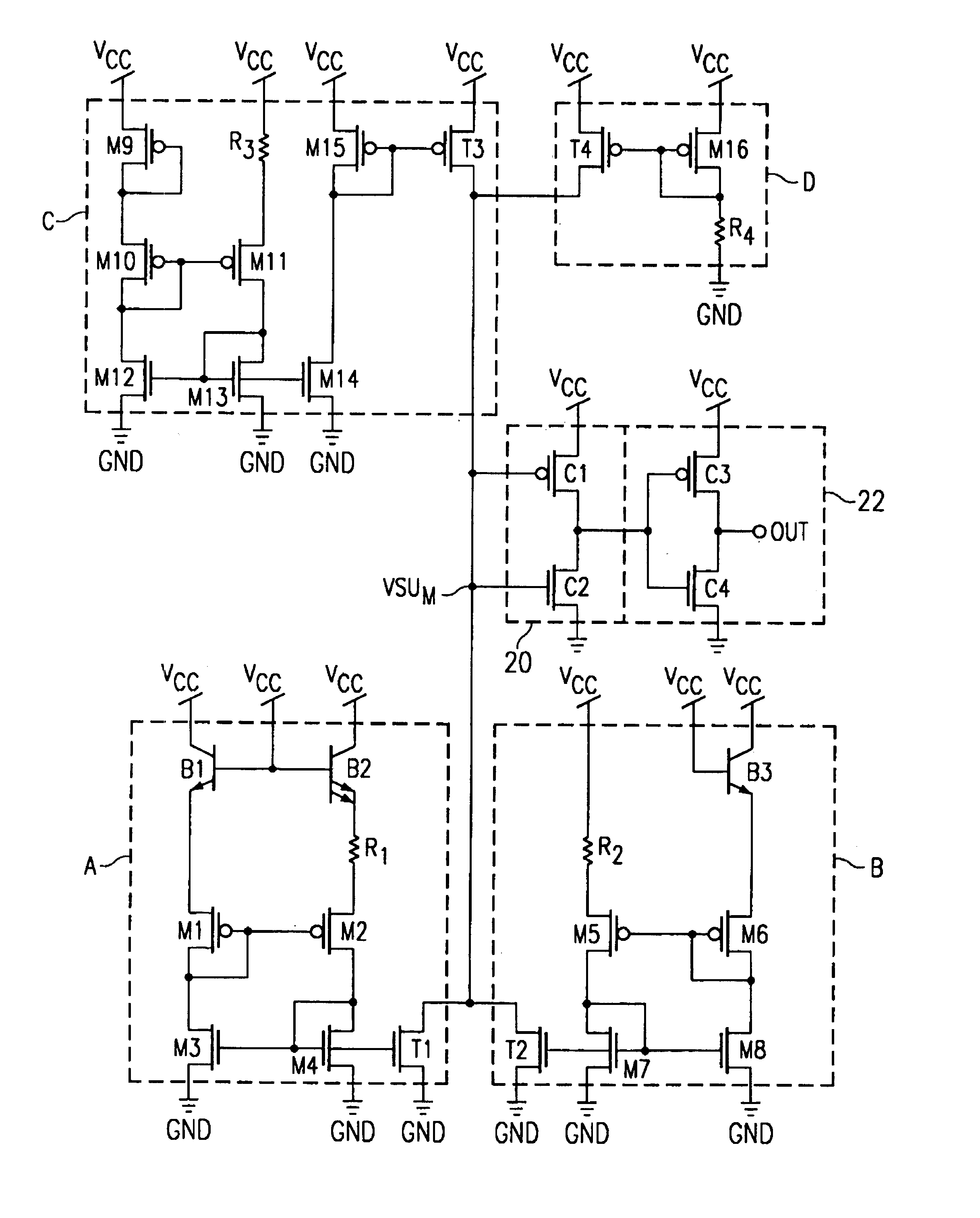
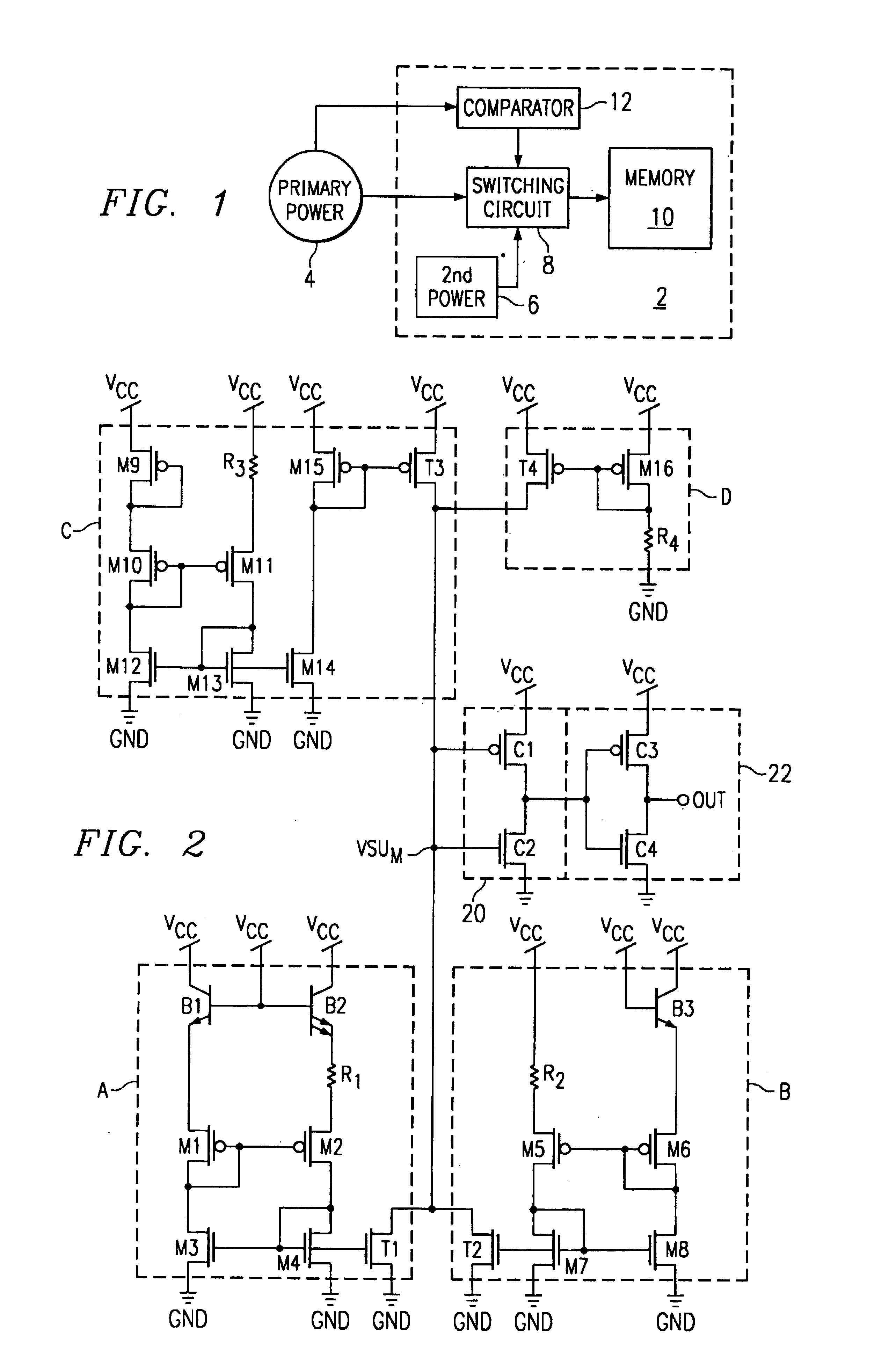
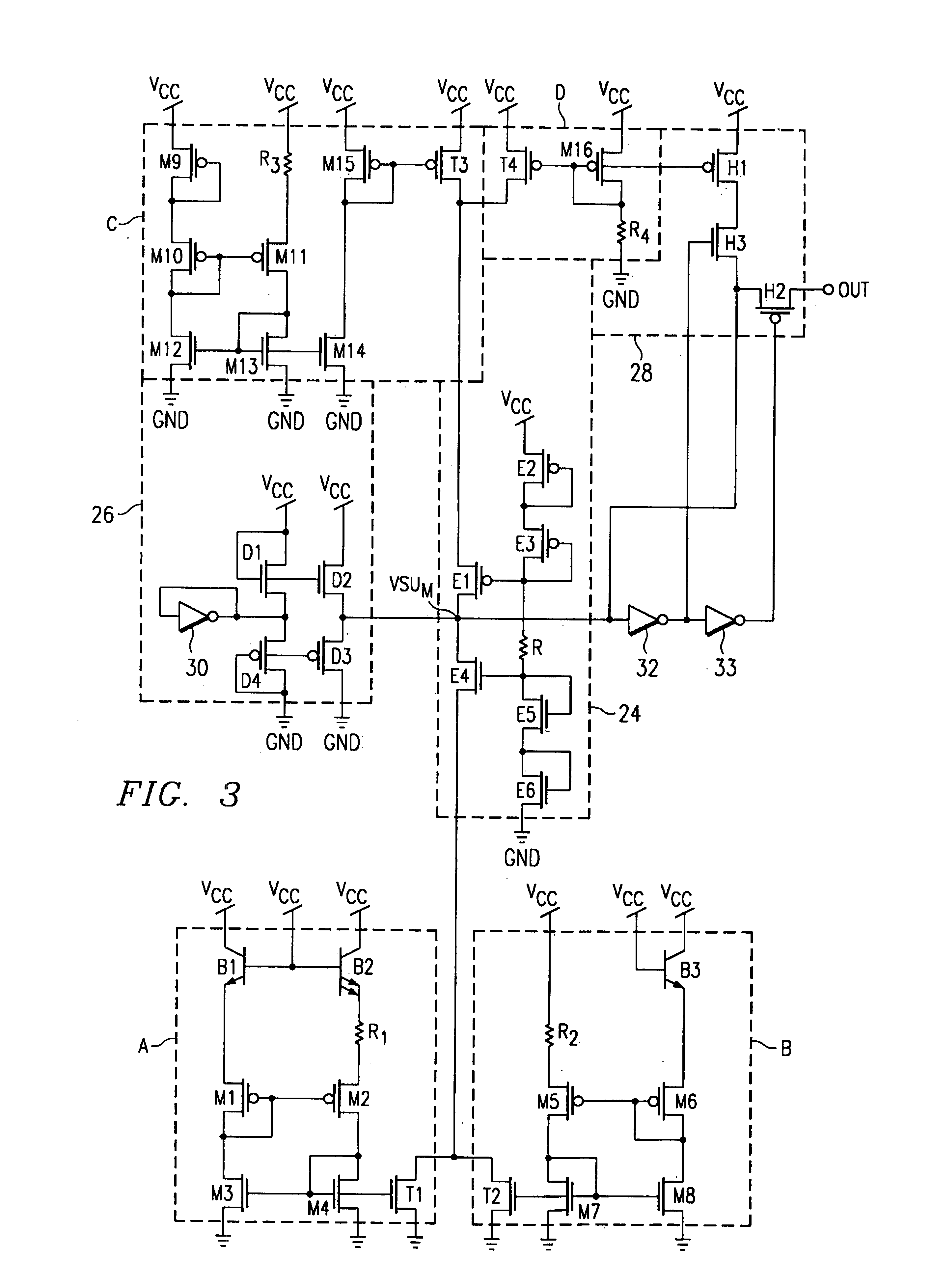
[0015]Referring now to FIG. 1, a block diagram of a zero power circuit 2 on a chip is illustrated. Zero power circuit 2 is connected to a primary power supply 4 and has a secondary power supply 6, located within an integral package. Secondary power supply 6 is typically a battery constructed in the plastic package housing the chip. Other secondary power supplies, such as, for example, a battery located outside the package may also be used.

[0016]Zero power circuit 2 includes a switching circuit 8, a memory 10, and a direct current sum bandgap voltage (DCSBV) comparator 12 constructed according to the present invention. Switching circuit 8 is connected to primary power supply 4 and secondary power supply 6. This circuit controls the power supplied to memory 10 and may include logic to provide for continuous supply of power to memory 10 during switching back and forth between primary power supply 4 and secondary power supply 6.

[0017]DCSBV comparator 12 has an input connected to primary...


PUM


Abstract

A direct current sum bandgap voltage comparator for detecting voltage changes in a power supply. The direct current sum bandgap voltage comparator includes a summing node, current sources connected to the summing node and the power supply, and an indicator circuit connected to the summing node. Each current source supplies a current to the summing node wherein the summing node voltage level is responsive to the currents supplied. The indicator circuit is responsive to changes in the summing node voltage level and generates at an output a logical signal at one state when the summing node voltage level is greater than a predetermined value and generates the logical signal at the output at another state when the summing node voltage level is less than the predetermined value, the predetermined value corresponding to a preselected power supply voltage.

Description

[0001]This is a Continuation of application Ser. No. 08 / 606,233, filed Feb. 23, 1996, now abandoned, which is a Continuation of application Ser. No. 08 / 056,301, filed Apr. 30, 1993, now abandoned.BACKGROUND OF THE INVENTION[0002]1. Field of the Invention[0003]The present invention relates to integrated circuits and in particular to MOS integrated circuits. Still more particularly, the present invention relates to bandgap reference circuits in insulated gate FET semiconductor integrated circuits.[0004]2. Description of the Prior Art[0005]In some situations it is desirable to provide retention of data in integrated circuits such as memory devices. A number of circuits are commercially available for retaining data in SRAMS when power is removed. These devices are often known as “zero power circuits”. Typically, in a zero power circuit, the contents of the circuit are protected in the event that the power supply voltage to that circuit drops below some predetermined or preselected thres...

Claims


Application Information

Patent Timeline
Patent Type & Authority Patents(United States)
IPC IPC(8): H03K5/22G01R19/165G05F3/24G05F3/26G05F3/30G11C5/14G11C11/413
CPCG01R19/16538G05F3/24G05F3/262G05F3/30G11C5/141G11C5/143
Inventor SLEMMER, WILLIAM CARL
Owner STMICROELECTRONICS SRL
Why Eureka
Try Eureka