
Micro-full analytical system chip height positioning method

A technology of system chip and positioning method, which is applied in the direction of material analysis, material analysis through optical means, microstructure technology, etc., can solve problems such as high cost, high technical requirements for adjustment personnel, and high technical difficulty, so as to ensure correct positioning Effect

Inactive Publication Date: 2008-01-02
SHANGHAI SPECTRUM INSTR
View PDF5 Cites 0 Cited by
  • Summary
  • Abstract
  • Description
  • Claims
  • Application Information

AI Technical Summary

Problems solved by technology

[0005] ② Manual adjustment generally requires a microscope to cooperate, the adjustment is cumbersome and time-consuming, the technical requirements for the adjustment personnel are high, and the work efficiency is low
[0006] ③Automatic adjustment requires a complete system of drivers, detectors, signal discrimination, feedback, and control, which is technically difficult and expensive

Method used


Image

  • Micro-full analytical system chip height positioning method

Examples


Embodiment Construction

[0017] The present invention will be further described below in conjunction with drawings and embodiments.

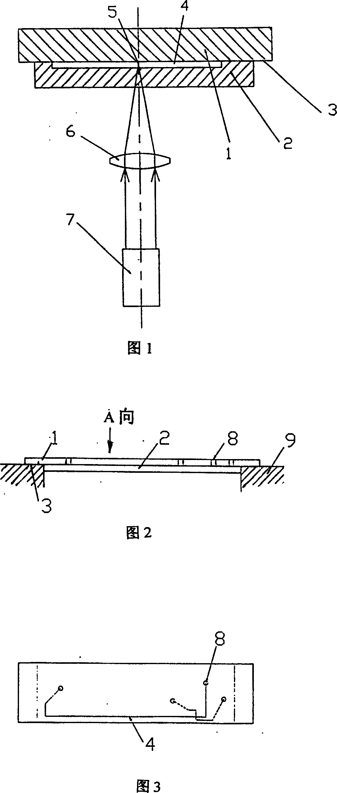
[0018] A micro total analysis system chip height positioning method:

[0019] 1) Adjust the height of the light source 7 and the chip workbench 9 with a standard chip (the channel position and size is fixed) when the instrument leaves the factory, so that the focal point 5 of the light source that can be observed when looking down is less than or equal to the width of the microchannel 4;

[0020] 2) the working chip comprises a cover sheet 1 and a substrate 2, the cover sheet 1 is engraved with an aperture 8, the upper surface of the substrate 2 is engraved with a microchannel 4, and the cover sheet 1 and the substrate 2 are bonded, The upper surface of the substrate 2 is closely attached to the lower surface of the cover sheet 1, and the small holes 8 communicate with the corresponding microchannels 4 respectively, and the area of ​​the cover sheet 1 is greater than th...


PUM


Abstract

A CMOS chip height location method of micro entire analysis system: uses the standard chip to adjust the height of the light source and the chip working table, the seeable focus point of the light source is smaller or equal to the width of the micro-channel when looking downward; the working chip includes the covering slice and the base slice, the top surface of the base slice bond and the bottom surface of the covering slice joint close by the bonding method, the holes chisels on the covering slice, the micro-channel chisels on the top surface of the base slice, the hole connects with the corresponding micro-channel, the area of the covering slice is bigger than the area of the base slice, forming the working chip sets on the support location surface of the chip working table in order that the support location surface of the covering slice touches with the table-board of the chip working table. The invention can avoid height location error leading by the thickness difference of the chip because of the difference of the material or the processing technology.

Description

technical field [0001] The invention relates to a height positioning method for a miniature total analysis system chip. Background technique [0002] The miniature full analysis system is also called lab-on-a-chip, which integrates laboratory functions including sampling, dilution, reagent addition, reaction, separation, and detection on the chip. Small holes are carved on the surface of the chip, and microchannels are carved in the chip. Small holes are used to store samples, reagents or waste liquid, and different channels are used for sample injection, reagent addition, reaction, separation and detection. In an analytical instrument composed of a chip, the absorption of the light source light by the reagent or sample in the chip, or the degree of excitation by the light source light, etc. are generally measured. Only when the focus point of the light source is exactly on the specific channel of the chip (ie, the microchannel), the light energy in the channel is the stro...

Claims


Application Information

Patent Timeline
Patent Type & Authority Patents(China)
IPC IPC(8): G02B7/00G01N21/00B81B7/00
Inventor 王鹗陈建钢方群刘志高王伟张涛富景林张大伟
Owner SHANGHAI SPECTRUM INSTR
Features
  • Generate Ideas
  • Intellectual Property
  • Life Sciences
  • Materials
  • Tech Scout
  • Unparalleled Data Quality
  • Higher Quality Content
  • 60% Fewer Hallucinations
Learn More