Semiconduetor storage device based on pseudo-unit method

A semiconductor and pseudo-cell technology, applied in the field of semiconductor storage devices based on the pseudo-cell method, can solve problems such as fluctuations and data read tolerance reduction

Inactive Publication Date: 2008-02-13
SOCIONEXT INC
View PDF4 Cites 0 Cited by
  • Summary
  • Abstract
  • Description
  • Claims
  • Application Information

AI Technical Summary

Problems solved by technology

As a result, the reference potential used for the data read operation fluctuates according to the access interval, thereby causing a problem of reduction of the data-read margin (data-read margin)

Method used


Image

  • Semiconduetor storage device based on pseudo-unit method
  • Semiconduetor storage device based on pseudo-unit method
  • Semiconduetor storage device based on pseudo-unit method

Examples


Embodiment Construction

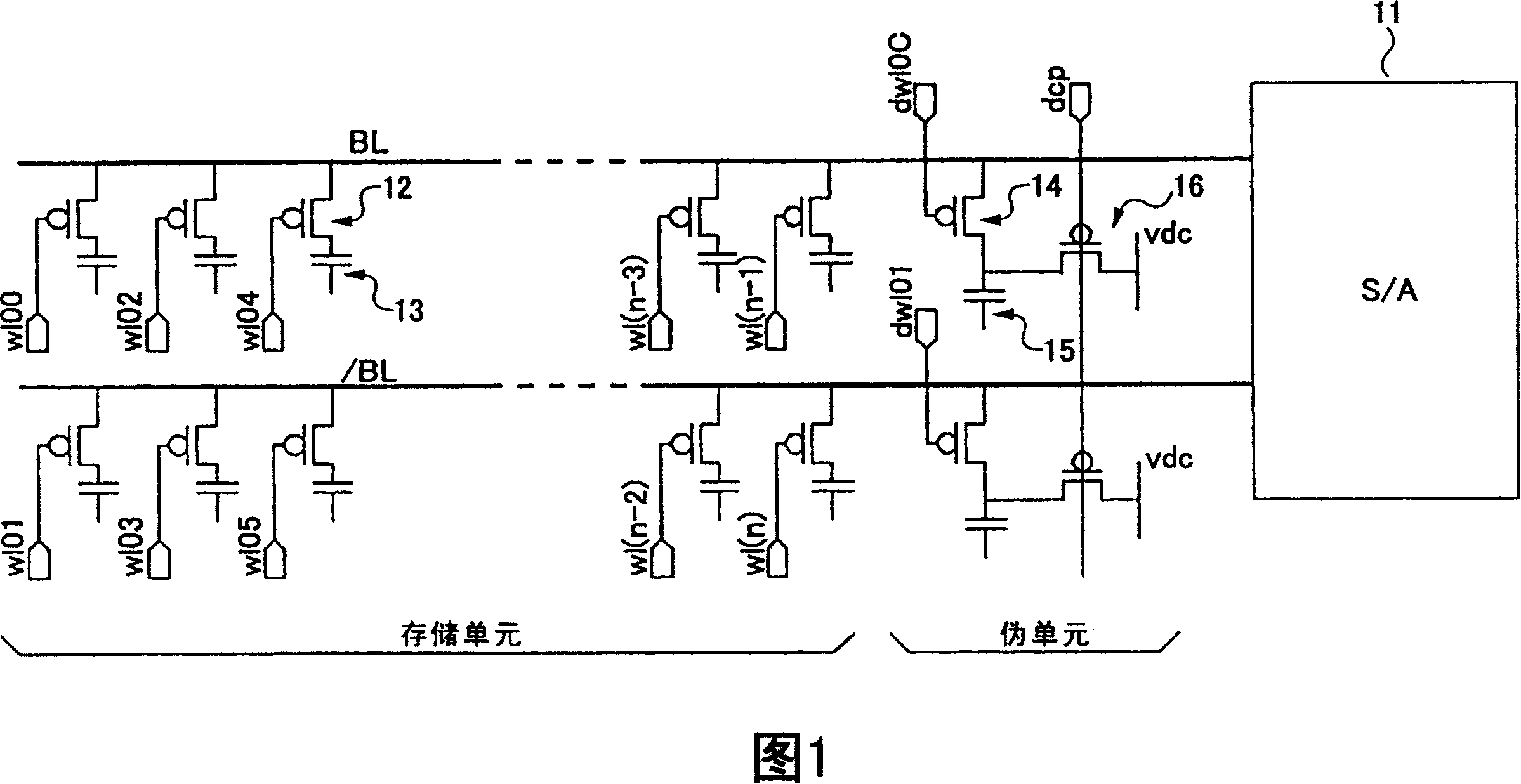
[0031] Embodiments of the present invention will be described below with reference to the accompanying drawings.

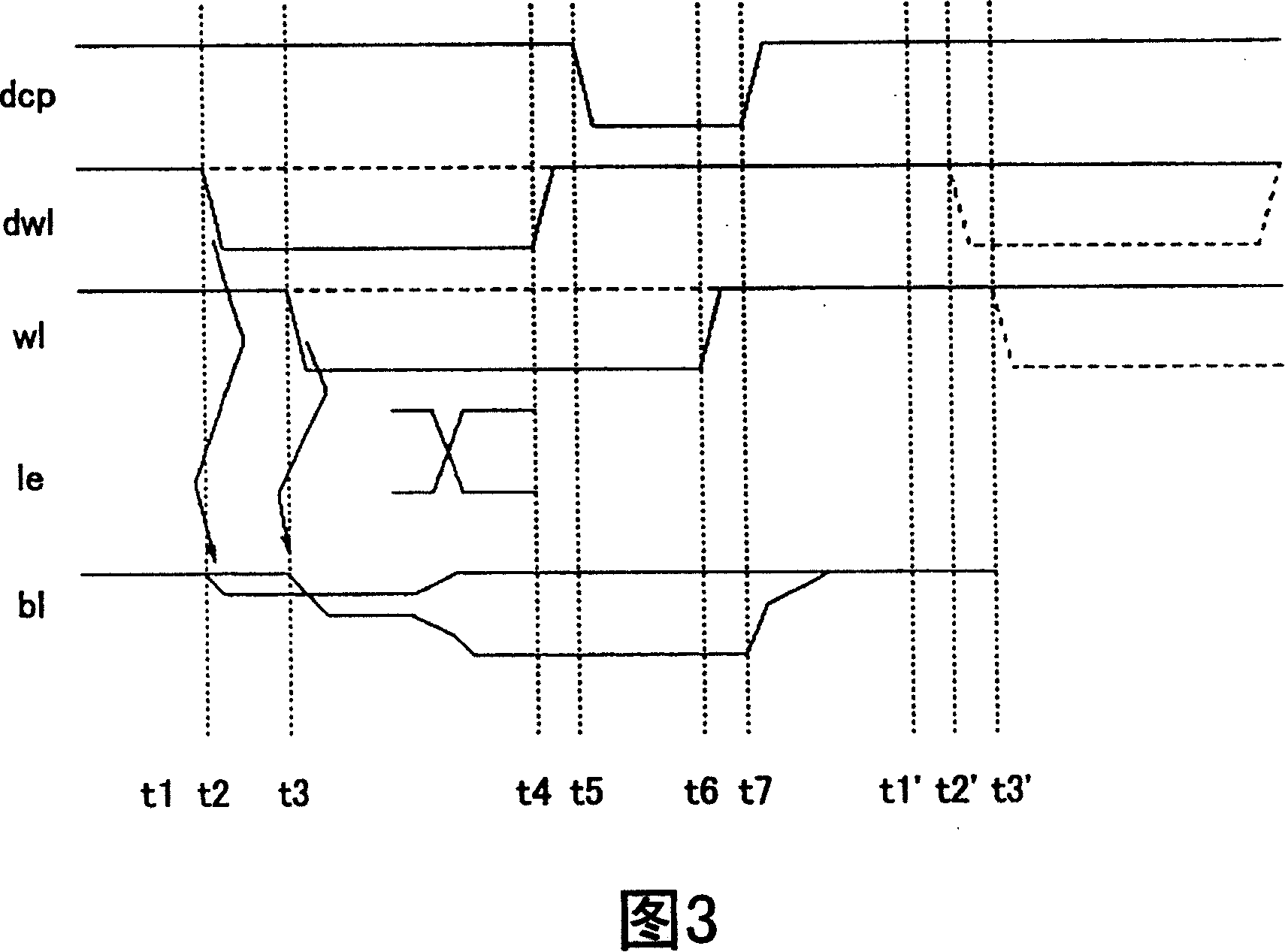
[0032] FIG. 3 is a timing chart for explaining the basic operation of dummy cell precharging according to the present invention.

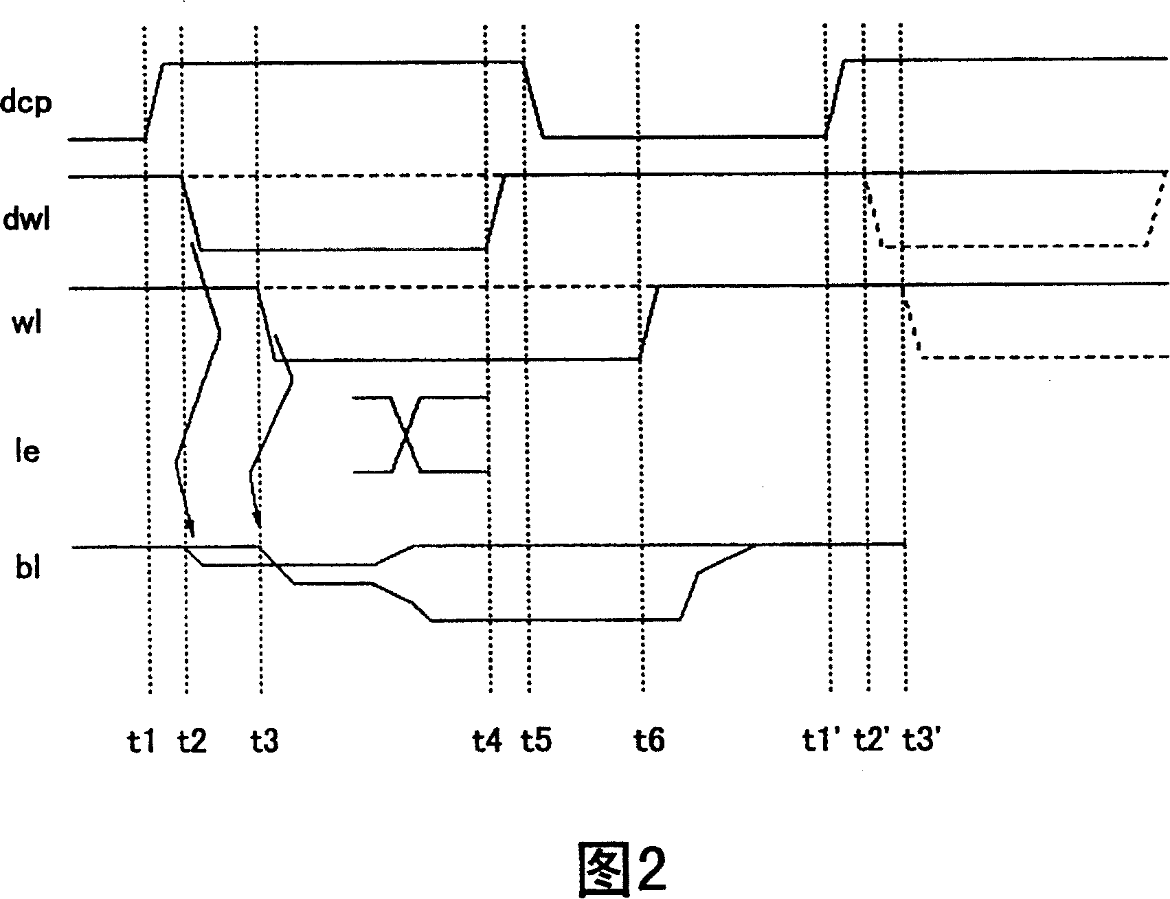
[0033] In the timing diagram of the related art read operation shown in FIG. 2, the dummy cell precharge line dcp is kept in an active state to precharge the dummy cells until time t1, wherein time t1 comes immediately before time t2, and at time t2 The dummy word line dw1 is activated to start an access operation. In addition, the dummy cell pre-charging line dcp is activated to start precharging the dummy cells at time t5, wherein the time t5 comes immediately after time t4, and the dummy word line dw1 is deactivated at time t4. Thereafter, the precharging of the dummy cells continues until the next access is performed.

[0034] On the other hand, in the dummy precharging operation of the present invention as shown in FIG. 3, at ti...


PUM


Abstract

A semiconductor memory device includes a plurality of bit line pairs, each of which includes a first bit line and a second bit line, a plurality of memory cells which are coupled to said first bit line, and store electric charge in capacitors, a dummy cell which is coupled to a second bit line, and is charged with a predetermined potential, a sense amplifier which amplifies a potential difference between the first bit line and the second bit line, and a control circuit which charges said dummy cell with the predetermined potential only for a fixed time period.

Description

technical field [0001] The present invention relates generally to semiconductor memory devices, and more particularly to semiconductor memory devices operating based on a pseudo-cell method. Background technique [0002] In DRAM (Dynamic Random Access Memory), a pair of bit lines are precharged to a potential midway between the power supply potential and ground potential, then data is read to one bit line, and the paired bits are then amplified by using a sense amplifier The potential difference between the wires is used to read the data. As the power supply potential has decreased in recent years, it has become increasingly difficult to generate a stable intermediate potential between the power supply potential and the ground potential. Therefore, some technologies using the power supply potential or the ground potential as the pre-charging potential have been developed. Methods of reading data in these technologies include pseudo-cell methods. [0003] FIG. 1 is a circu...

Claims


Application Information

Patent Timeline
Patent Type & Authority Patents(China)
IPC IPC(8): G11C11/401G11C7/12G11C11/403G11C7/06G11C7/14G11C11/406G11C11/4091G11C11/4099
CPCG11C11/4091G11C7/062G11C7/14G11C11/4099G11C7/12
Inventor 泷田雅人山田伸一松宫正人
Owner SOCIONEXT INC
Why Eureka
Try Eureka