

Semiconductor device
A semiconductor and MOS transistor technology, applied in the driving field of semiconductor devices, can solve problems such as steep threshold value changes between circuits, unfixable output, and readout errors
- Summary
- Abstract
- Description
- Claims
- Application Information
AI Technical Summary
Problems solved by technology
Method used
Image

Examples
no. 1 example
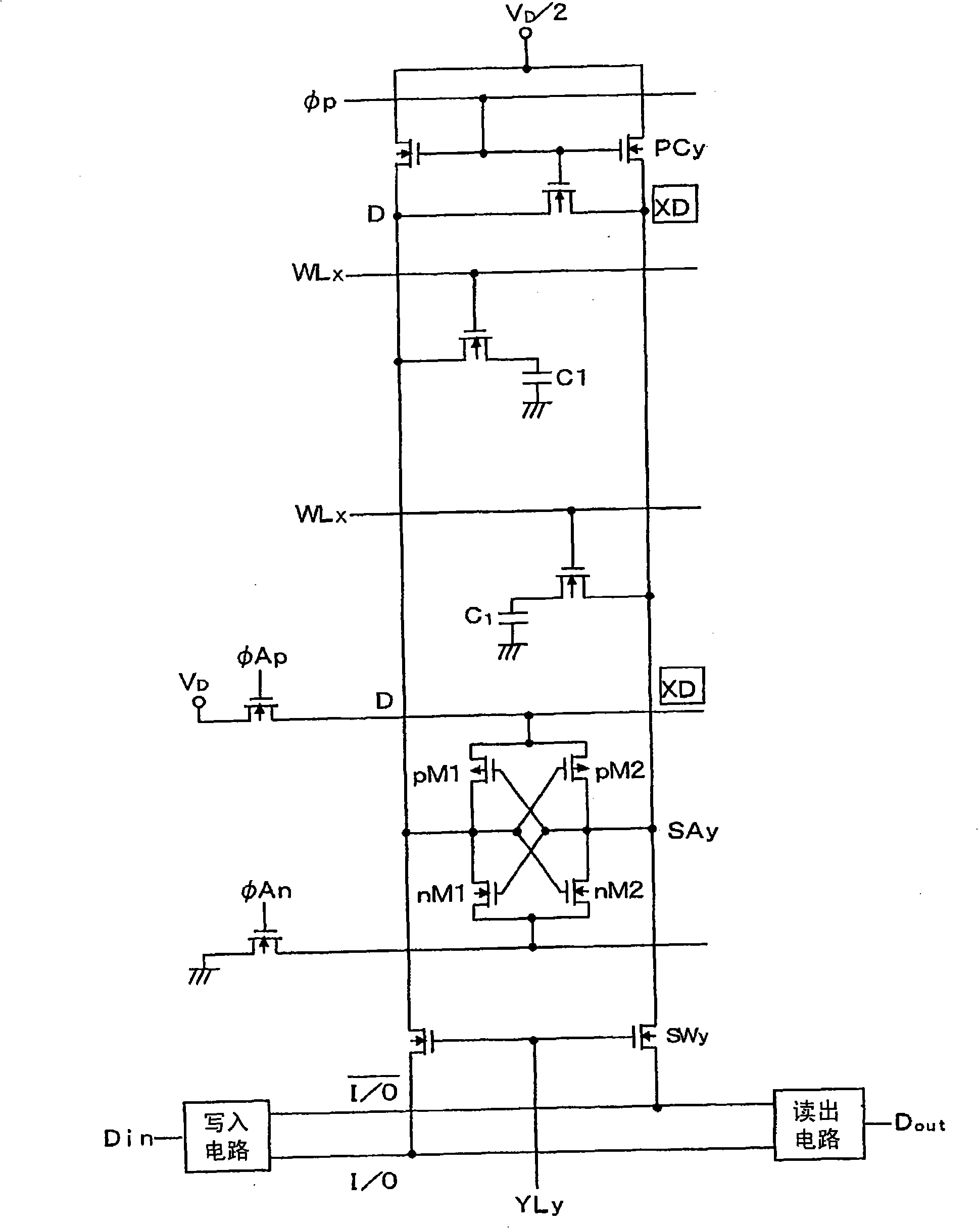
[0314] FIG. 16 is a flowchart showing a method for driving the latch circuit according to the first embodiment of the present invention. The latch circuit used to explain this driving method is the same as Figure 11 The illustrated latch type sense amplifier circuit composed of n-channel MOS transistors is the same. That is, the latch circuit of the present invention includes a polysilicon TFT N1 (4901a) and a transistor N2 (4901b) whose sources are commonly connected. The gate of TFT N1 is connected to the drain of transistor N2, and is also connected to capacitor C2. The gate of TFT N2 is connected to the drain of transistor N1, and is also connected to capacitor C1.
[0315] The latch circuit is driven as follows: In the first period (active period) (5001), using the electrical characteristics of the MOS transistors (4901a and 4901b), signals necessary for circuits other than the latch circuit not shown are output, And in the second period (idle period) (5002), a reset ...
no. 2 example
[0406] Although the example in which the VDS of the MOS transistor is 0 and no current flows when the body potential reset pulse is applied has been shown in the first embodiment, the same circuit as in the first embodiment is used in the second embodiment of the present invention ( Such as Figure 11 circuit shown), and perform a different drive from Figure 16.
[0407] FIG. 26 is a flowchart showing a method for driving the latch circuit of the present invention. It differs from FIG. 16 in that (VDD1-Vt)V is supplied to node K during the period in which the body potential reset pulse is applied, so that drain current flows into the MOS transistor to which the body potential reset pulse is being input.
[0408] Here, although (VDD1−Vt)V supplied to the node K has been described, it is also a voltage set conveniently for using the circuit of FIG. 17 in an experiment, and therefore, simply applying VDD1 is substantially the same.
[0409] The latch circuit is driven as follows:...
no. 3 example
[0431] In this embodiment, a description will be given of a specific example of a latch type sense amplifier circuit to which the driving method of the first embodiment is applied.
[0432] A circuit diagram of the sense amplifier circuit of the present invention is shown in Fig. 28A. The transistor N1 (4901a) and the transistor N2 (4901b) are n-channel polysilicon TFTs, and the transistor N3 is for switching on and off the connection between the source (node K) of the transistors N1 and N2 and the SAN electrode according to the signal SE3. Part of the n-channel polysilicon TFT. The SAN nodes are connected to VSS (eg, 0V).
[0433] Denoted node A is for the drain of transistor N1, and denoted node B is for the drain of transistor N2. Bit line ODD (5301a) is connected to node A through switch M03 (4905a), and the on / off of switch M03 (4905a) is controlled by PAS. In addition, bit line EVN (5301b) is connected to node B through a transfer control part (ie, switch M04) (4905...
PUM
 Abstract
Description
Claims
Application Information