Active component array substrate
An array substrate and active element technology, applied in the field of active element array substrates, can solve problems such as display unevenness, and achieve the effect of reducing impedance gap and improving display unevenness.
- Summary
- Abstract
- Description
- Claims
- Application Information
AI Technical Summary
Problems solved by technology
Method used
Image
Examples
no. 1 example
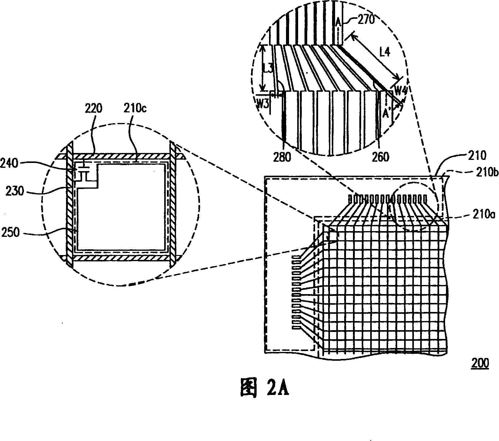
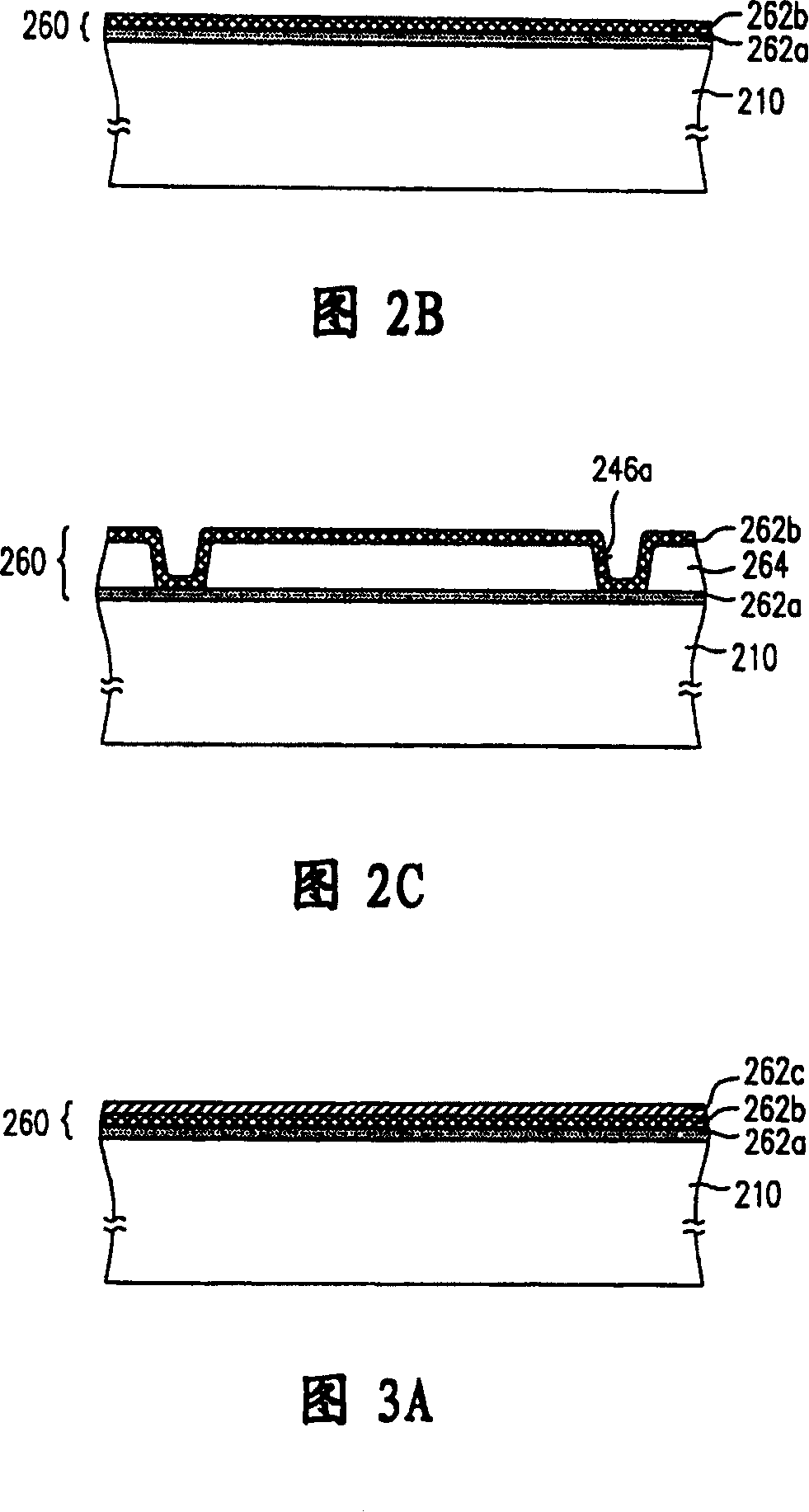
[0038] FIG. 2A shows a top view of an active device array substrate according to a first preferred embodiment of the present invention, and FIG. 2B shows a cross-sectional view along line A-A' of FIG. 2A. Please refer to FIG. 2A and FIG. 2B at the same time. The active element array substrate 200 of this embodiment includes a substrate 210, a plurality of scanning wiring lines 220, a plurality of data wiring lines 230, a plurality of switching elements 240, a plurality of pixel electrodes 250, A plurality of first traces 260 , a plurality of second traces 280 and a plurality of bonding pads 270 , wherein the substrate 210 defines a display area 210 a and a non-display area 210 b. In addition, the scan wires 220 and the data wires 230 are disposed on the display area 210 a, and the scan wires 220 and the data wires 230 define a plurality of pixel areas 210 c on the substrate 210 . In addition, the switching elements 240 are respectively disposed on the pixel area 210c, wherein ...
no. 2 example
[0048] 3A to 3E are cross-sectional views of the first trace according to the second preferred embodiment of the present invention. Please refer to FIG. 3A, FIG. 3A is similar to FIG. 2B, the difference is that: in order to further reduce the impedance, the first wiring 260 further includes a third conductor layer 262c, which is disposed on the second conductor layer 262b, and the first The conductor layer 262a, the second conductor layer 262b and the third conductor layer 262c are electrically connected in parallel. In this embodiment, the first conductor layer 262a and the scan wiring 220 may be the same film layer, the second conductor layer 262b and the data wiring 230 may be the same film layer, and the third conductor layer 262c and the pixel electrode 250 may be are the same layer.
[0049] Please refer to FIG. 3B . FIG. 3B is similar to FIG. 2C except that: after the second conductor layer 262 b is formed, a third conductor layer 262 c is formed on the second conducto...
PUM
 Abstract
Description
Claims
Application Information


