Supercharge Your Innovation With Domain-Expert AI Agents!

High speed zero DC power programmable logic device (PLD) architecture

A technology for programming logic and devices, applied in logic circuits, logic circuits using basic logic circuit components, and electro-solid devices, etc., and can solve problems such as sense amplifier consumption, high power, and incorrect PLD reading.

Inactive Publication Date: 2008-02-13
ATMEL CORP
View PDF9 Cites 0 Cited by
  • Summary
  • Abstract
  • Description
  • Claims
  • Application Information

AI Technical Summary

Problems solved by technology

In addition, the sense amplifiers consume a considerable amount of power in normal operation
Also, noise spikes (spikes) often cause the PLD to read incorrect values ​​to its output logic

Method used


Image

  • High speed zero DC power programmable logic device (PLD) architecture
  • High speed zero DC power programmable logic device (PLD) architecture
  • High speed zero DC power programmable logic device (PLD) architecture

Examples


Embodiment Construction

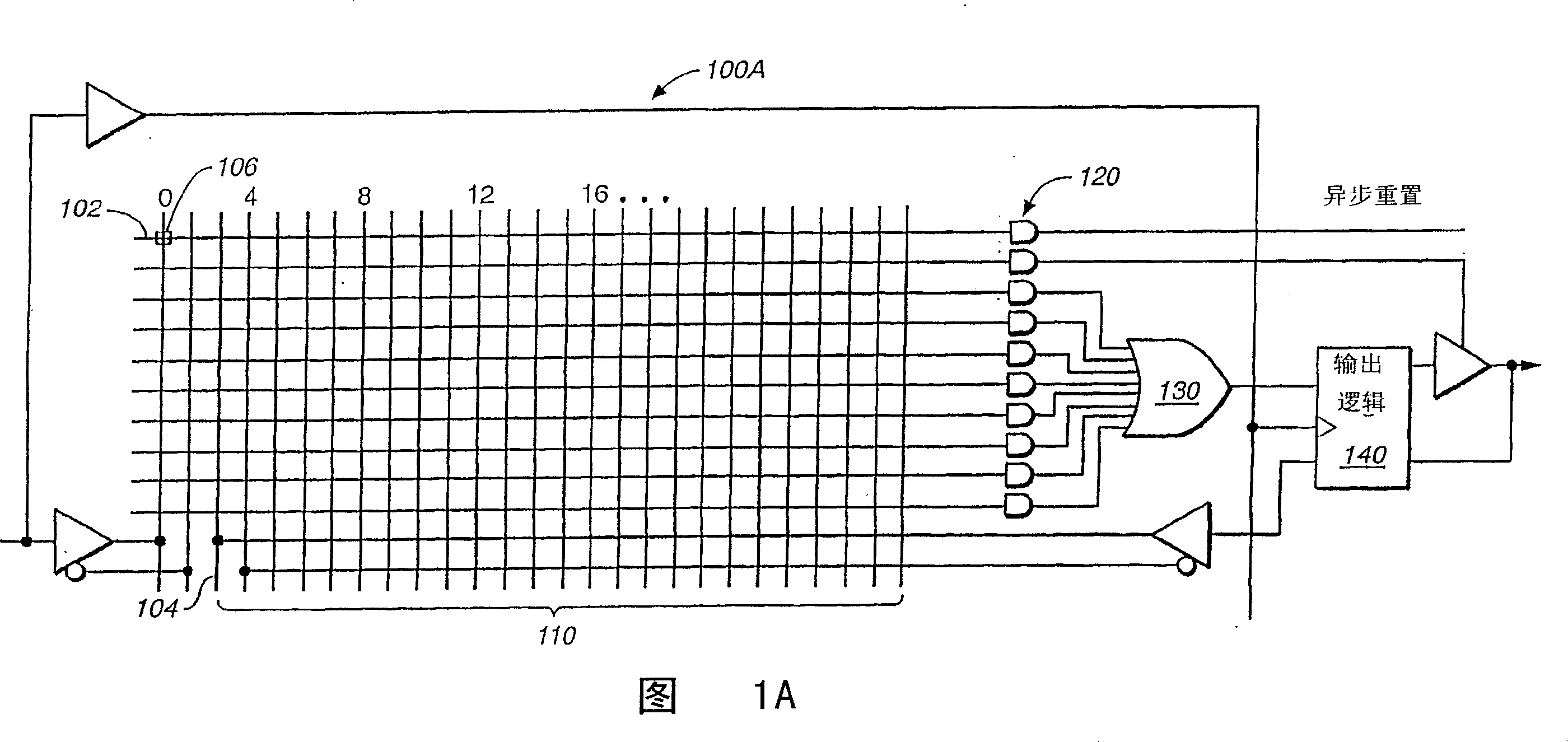
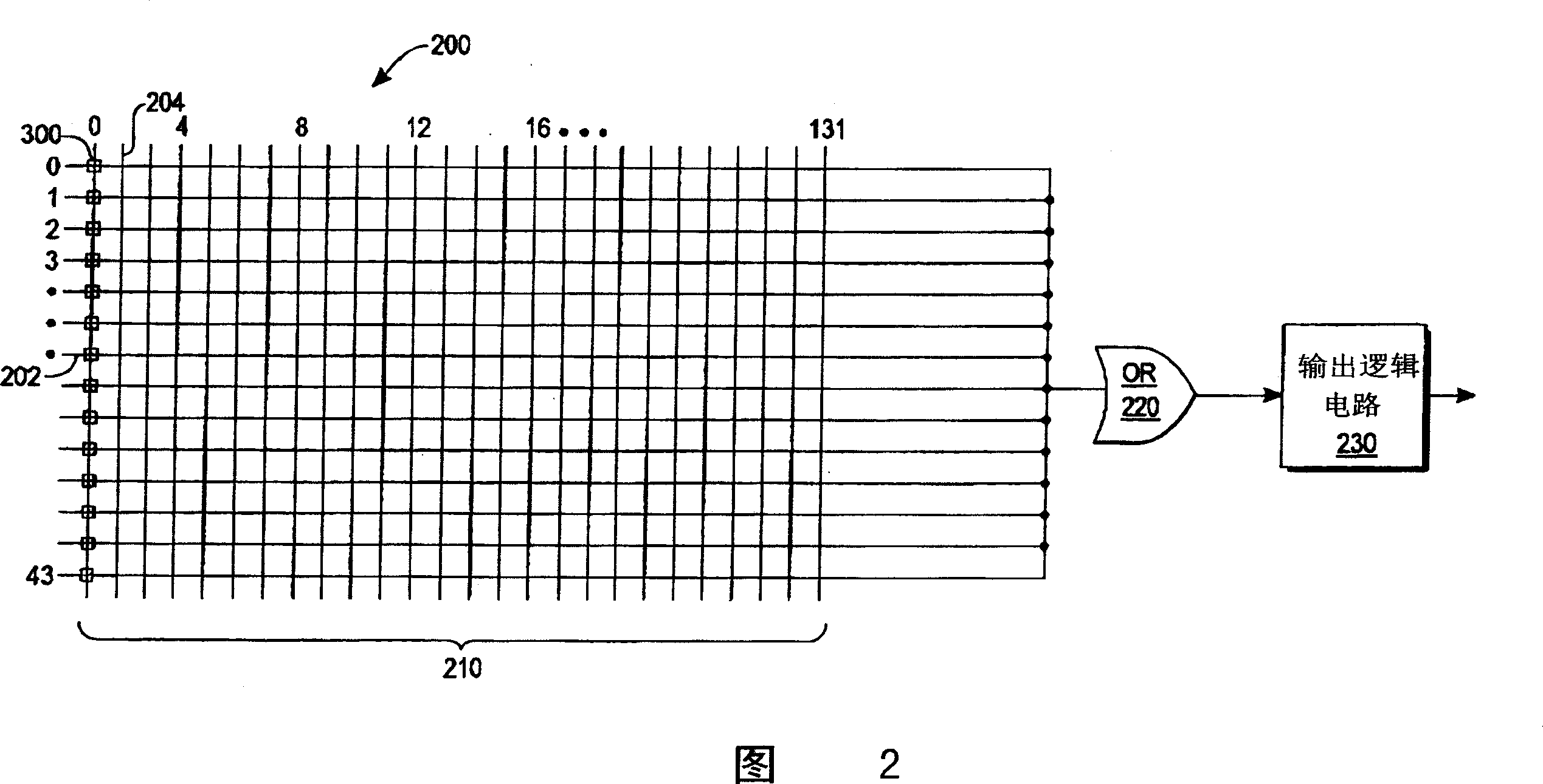
[0023] Referring to FIG. 2 , a new PLD structure 200 is implemented by using PLD unit cells as basic building blocks to construct a programmable array. The PLD structure 200 has a programmable array 210 , an array of OR gates 220 and an output logic circuit 230 like any prior art PLD. However, the programmable array 210 of the PLD 200 is configured by using a plurality of PLD unit cells 300 . The PLD unit cell 300 will be described in detail later with reference to FIG. 3 . In a preferred embodiment, the PLD structure 200 has 44 rows and 132 columns.

[0024]In FIG. 2 , each PLD unit cell 300 is represented by a square located at the intersection of each row 202 and each column 204 . The total number of rows 202 and columns 204 of PLD unit cells 300 in a PLD device is a matter of design choice and may vary according to user needs. The PLD structure 200 in FIG. 2 is an example with 5808 cells arranged in a programmable array 210 having 44 rows and 132 columns. Each column 2...


PUM


Abstract

A programmable logic device (PLD) architecture includes a plurality of PLD single-bit logic cells (Fig.3). Each single bit logic cell is comprised of all CMOS logic devices including a programmable cell unit (330-333), a settable latch (320-323), a signal path means (360A, 360B), and an output logic gate (350). The signal-path means coupled to the cell unit, the settable latch, and the output logic gate to create a positive feedback loop to improve speed and noise immunity. Each single bit logic gate is a basic building block (402-408) for a modular low power consumption, high speed, zero DC current, high noise immunity programmable logic device (PLD) (700) which includes an array of word lines (pwd) and bit lines (vcol, pcol) arranged in rows and columns for addressing, an array of OR gates (740), and a plurality of output logic circuits (750).

Description

field of invention [0001] The present invention generally relates to programmable logic devices (PLDs), and more particularly, the present invention relates to high-speed, zero DC power consumption PLD structures. Background of the invention [0002] Programmable logic devices (PLDs) are well known in the art and are widely used to perform complex digital logic functions in the form of sums of products or products of sums. Each PLD basically includes a memory array or matrix functioning as programmable AND gates, readout circuitry, a fixed OR gate array, and output logic circuitry. The array of fixed OR gates can also be a programmable OR array. When the row and column decoders select a particular cell to read or write data from, the sense amplifier in the sense circuit reads information from the selected cell, the fixed OR array, and the output logic circuit to perform logic functions. When this occurs, the bit line connected to the programmable array of the selected cell...

Claims


Application Information

Patent Timeline
Patent Type & Authority Patents(China)
IPC IPC(8): H03K19/177G11C16/04G11C16/26
CPCH03K19/17728H03K19/1778G11C16/0433H03K19/17704G11C16/26H03K19/1776H03K19/17784H01L25/00H03K19/177
Inventor 萨罗杰·帕塔克詹姆斯·E·佩恩V·V·恩古耶H·H·库
Owner ATMEL CORP
Features
  • R&D
  • Intellectual Property
  • Life Sciences
  • Materials
  • Tech Scout
  • Unparalleled Data Quality
  • Higher Quality Content
  • 60% Fewer Hallucinations
Learn More