Check patentability & draft patents in minutes with Patsnap Eureka AI!

Method for manufacturing component figure, distributing structure, and image display device

A manufacturing method and component technology, which can be used in the manufacture of discharge tubes/lamps, photoengraving processes of patterned surfaces, semiconductor/solid-state device manufacturing, etc., and can solve problems such as short circuits between wirings

Inactive Publication Date: 2008-02-27
CANON KK
View PDF6 Cites 0 Cited by
  • Summary
  • Abstract
  • Description
  • Claims
  • Application Information

AI Technical Summary

Problems solved by technology

However, in the multi-layer overlapping structure, there may be a short circuit between the wirings at the intersection of the X-direction wiring and the Y-direction wiring.

Method used


Image

  • Method for manufacturing component figure, distributing structure, and image display device
  • Method for manufacturing component figure, distributing structure, and image display device
  • Method for manufacturing component figure, distributing structure, and image display device

Examples


Embodiment approach 1

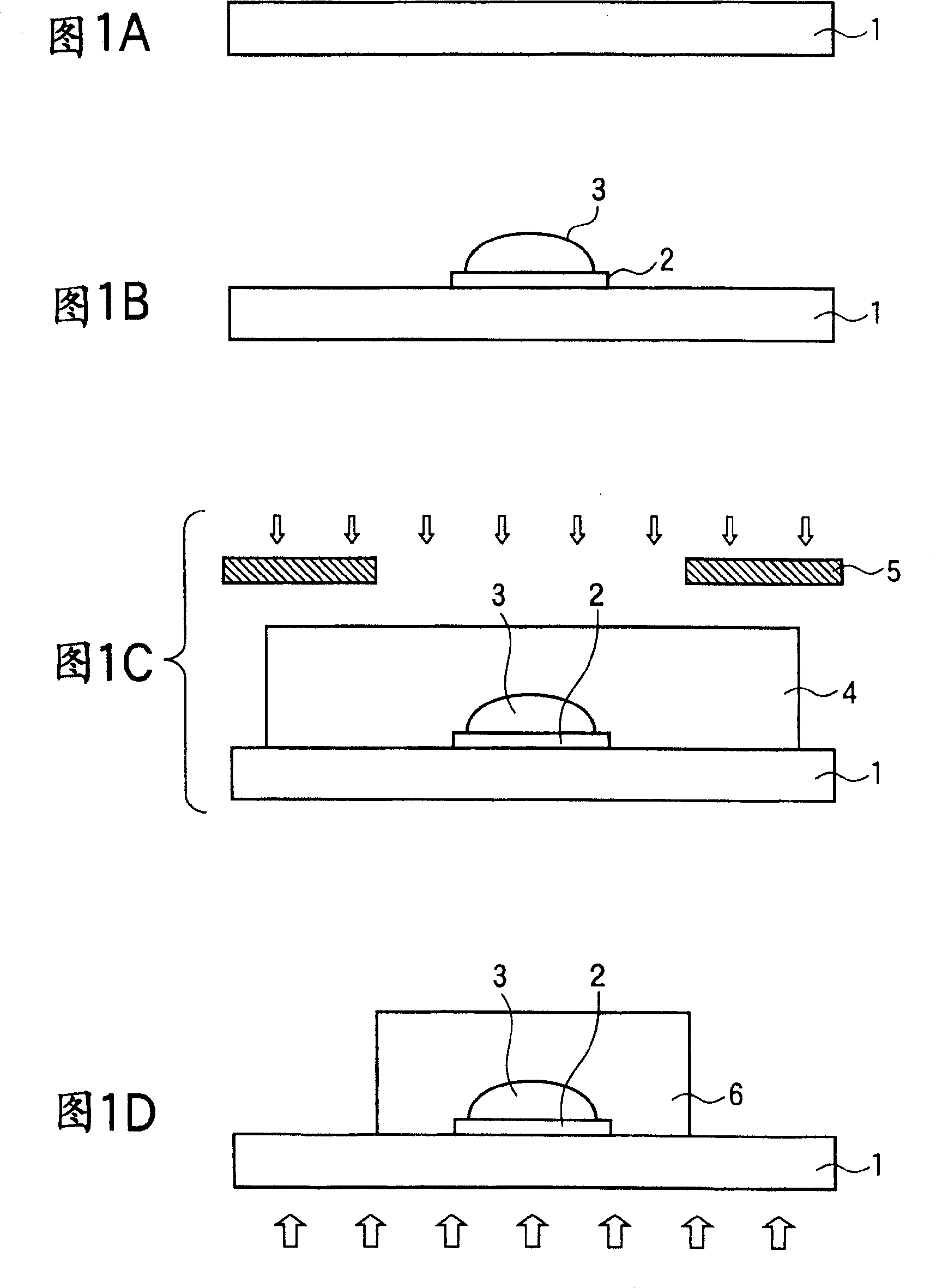
[0084] One embodiment of the method for forming an insulating film according to the present invention will be described with reference to FIG. 1 .

[0085] First, a translucent substrate 1 such as glass through which light for exposure can pass is prepared ( FIG. 1( a )).

[0086] Thereafter, if necessary, after forming the base layer 2 made of a conductor such as platinum, a conductive paste is applied by printing or the like, followed by firing. Thus, a wiring pattern 3 having a thickness of, for example, about 5 μm to 20 μm can be formed ( FIG. 1( b )). Here, the angle formed by the side surface of the wiring pattern 3 and the surface of the substrate 1 is an obtuse angle.

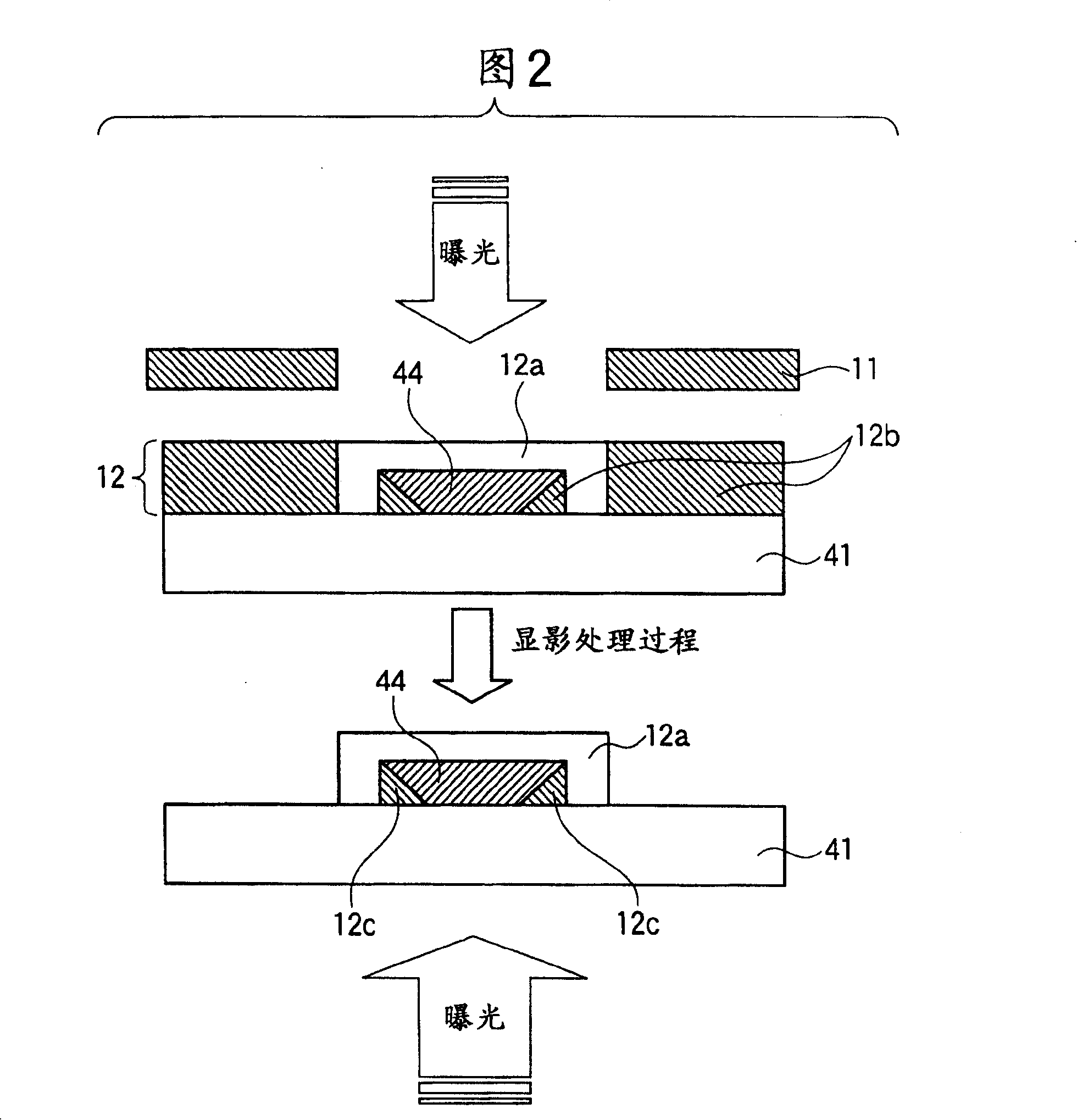
[0087] Thereafter, negative photosensitive insulating paste 4 is applied and dried by a printing method ( FIG. 1( c )). The film thickness after drying is, for example, about 10 μm to 40 μm. In addition, as the photosensitive insulating paste, well-known materials composed of, for example, 40% by vol...

Embodiment approach 2

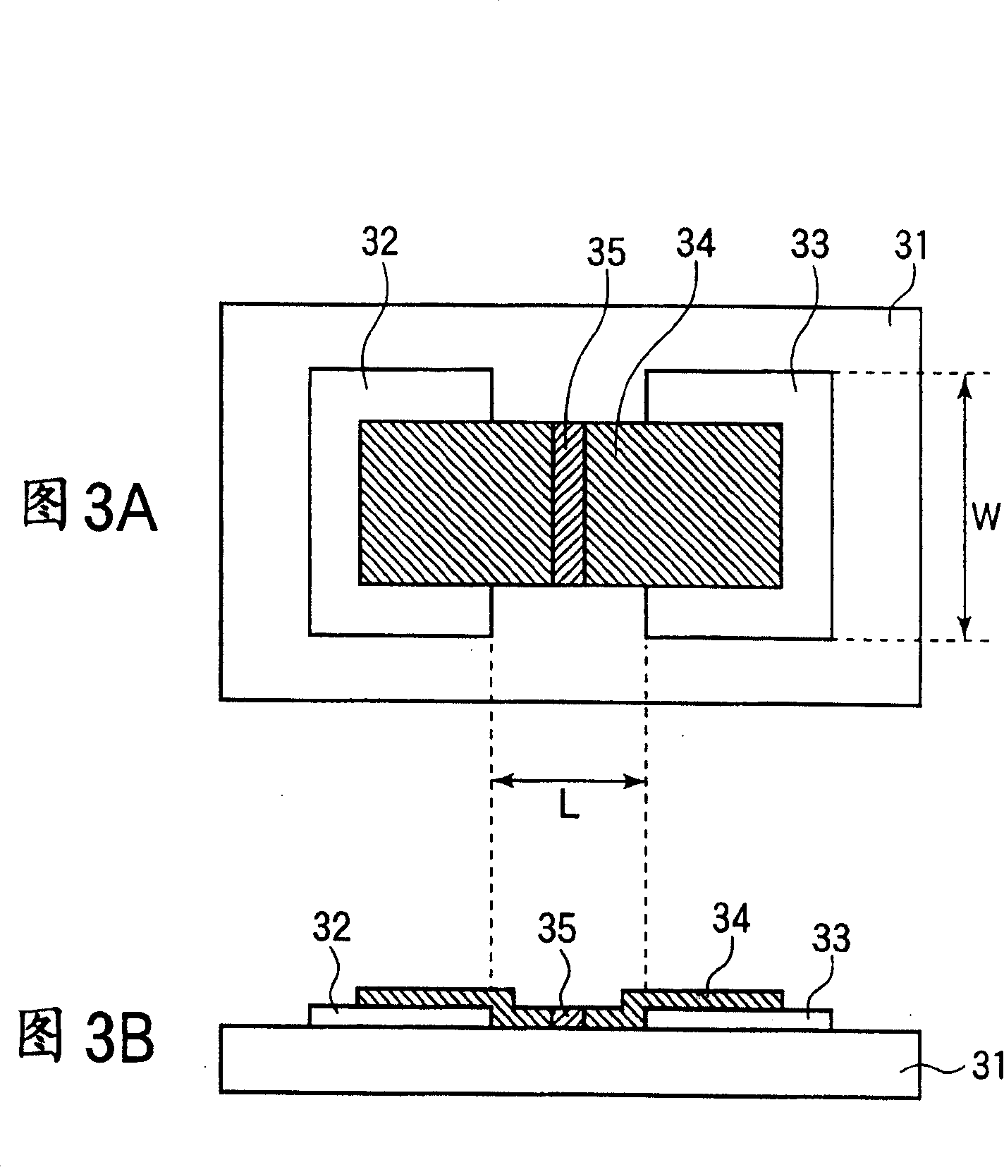
[0093] Next, as an example of application of the above-mentioned method of forming an insulating film according to a preferred embodiment of the present invention, centering on the electron source substrate shown in FIG. ,Be explained.

[0094] As the electron emission element formed on the electron source substrate of this embodiment, it is preferable to use a two-terminal type cold cathode that can be driven by a matrix. For example, a surface conduction type electron emission element and a horizontal type as shown in FIG. Field emission type electron emission element (FE), etc. Shown here is an example of formation of the surface conduction type electron emission element shown in FIG. 3 .

[0095] (Formation of device electrodes)

[0096] First, on a well-cleaned substrate 41, a plurality of element electrodes 42, 43 are arranged and formed by photolithography or the like (FIG. 4).

[0097] The substrate 41 is made of glass or the like, and its size and thickness can hol...


PUM

PropertyMeasurementUnit
thicknessaaaaaaaaaa
thicknessaaaaaaaaaa
diameteraaaaaaaaaa

Abstract

The present invention provides a method of manufacturing a member pattern having a patterned member on a substrate, the method including: a first exposure step of exposing a desired region of a negative type photosensitive material applied to the substrate to light from a first direction; a second exposure step of exposing the desired region of the negative type photosensitive material to light from a second direction opposite to the first direction; a development step of performing development after the exposure steps to form a precursor pattern of the member; and a step of baking the precursor pattern.

Description

technical field [0001] The present invention relates to a method of manufacturing a member pattern such as a wiring structure, and a method of manufacturing an electron source and an image display device using the same. Background technique [0002] The manufacturing method of the component pattern formed with the insulating film or the conductive film in the required pattern on the substrate is used in the manufacturing method of the wiring structure, and this wiring structure is applied to the plasma display (PDP), liquid crystal Display elements (LCD), field emission display elements (ELD), electron emission display elements, image display and imaging devices, etc. Hereinafter, an electron-emitting display element will be taken as an example for description. [0003] An electron emission element is disclosed in Japanese Patent Application Laid-Open No. 8-321254 and the like. Fig. 3(a) is a schematic plan view of a surface conduction type electron-emitting element, and F...

Claims


Application Information

Patent Timeline
Patent Type & Authority Patents(China)
IPC IPC(8): H01J9/00H01J9/02H01L21/027G03F7/00H01J1/304G02F1/1362G03F7/20
CPCH01J9/027G02F1/136286G03F7/2024G03F7/0035G03F7/2022H01J1/304
Inventor 山田修嗣蜂巢高弘目黒忠靖
Owner CANON KK
Features
  • R&D
  • Intellectual Property
  • Life Sciences
  • Materials
  • Tech Scout
  • Unparalleled Data Quality
  • Higher Quality Content
  • 60% Fewer Hallucinations
Learn More