Circuit arrangement

A circuit device and circuit technology, applied in the direction of lighting devices, electric light sources, electrical components, etc.

Inactive Publication Date: 2008-06-04
KONINKLIJKE PHILIPS ELECTRONICS NV
View PDF5 Cites 0 Cited by
  • Summary
  • Abstract
  • Description
  • Claims
  • Application Information

AI Technical Summary

Problems solved by technology

However, a disadvantage of this circuit arrangement is that not every value of the duty cycle o

Method used


Image

  • Circuit arrangement
  • Circuit arrangement
  • Circuit arrangement

Examples


Embodiment Construction

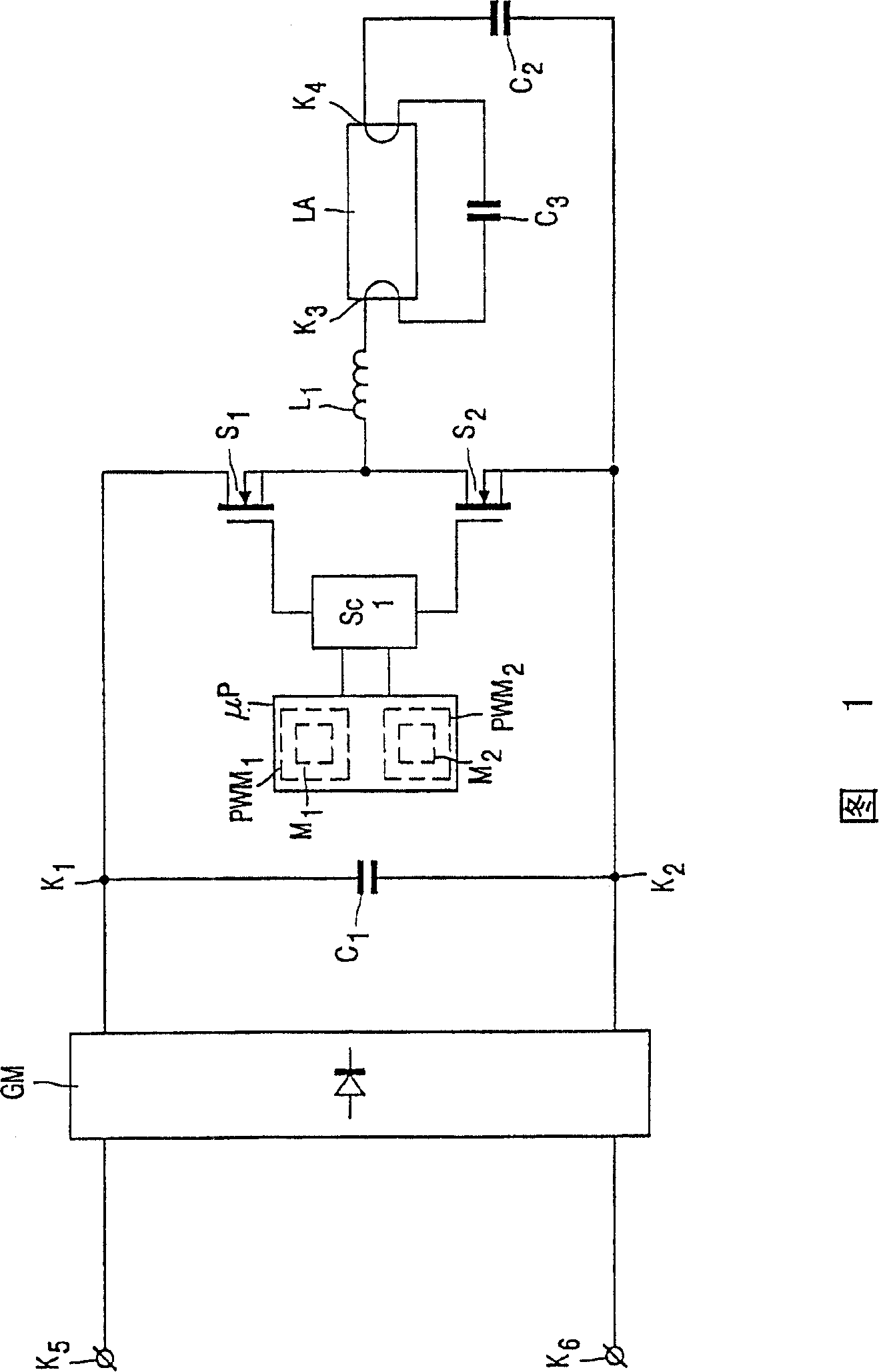
[0022] In FIG. 1, K5 and K6 indicate terminals that can be connected to the electrodes of an AC voltage source that provides a low-frequency AC voltage. K5 and K6 are respectively connected to the two input terminals of the rectifier device GM for rectifying the low frequency AC voltage. The two output terminals of the rectifier device GM are connected to the input terminals K1 and K2, while K1 and K2 are connected to a DC voltage source. The input terminal K1 is connected to the input terminal K2 through a capacitor C1. The DC voltage source is composed of an AC voltage source, a rectifier device GM, and a capacitor C1 as a buffer capacitor. The capacitor C1 is connected in parallel with the first switching element and the second switching element connected in series. The control electrode of the switching element S1 is connected to the first output terminal of the control circuit Sc. The control electrode of the switching element S2 is connected to the second output terminal of ...


PUM


Abstract

A ballast circuit comprises an inverter formed by a bridge circuit. The power consumed by a lamp connected to the ballast circuit is controlled by controlling the duty cycles of control signals that drive the bridge switches. The duty cycle is proportional to digital signals generated by a pulse duration modulator comprised in a microprocessor. To increase the number of settings to which the lamp power can be set, the digital signals are modulated.

Description

Technical field [0001] The invention relates to a circuit arrangement for energizing electric lamps, including: [0002] Connect to the input terminal of the DC voltage source; [0003] An inverter coupled to the input terminal, which generates lamp current from a DC voltage provided by a DC voltage source, the inverter includes: [0004] A switching element coupled to the input terminal; [0005] A control circuit coupled to the control electrode of the switching element, the control circuit is used to generate a control signal reflecting the alternate conduction and disconnection of the switching element; [0006] A pulse duration modulator, which is coupled to the control circuit and is used to set the duty cycle of the control signal, which is directly proportional to the digital signal appearing at the output of the pulse duration modulator. Background technique [0007] Such a circuit arrangement is well known. In this circuit arrangement, the duty cycle of the control sign...

Claims


Application Information

Patent Timeline
IPC IPC(8): H05B41/392H05B41/40
CPCH05B41/3921
Inventor M·贝A·W·布伊E·M·J·埃恩德克尔克W·H·M·兰格斯拉
Owner KONINKLIJKE PHILIPS ELECTRONICS NV
Why Eureka
Try Eureka