Magnetism integration DC/DC conversion boosting type transmission ratio expander circuit
A technology that expands the circuit and transmission ratio. It is applied in the direction of conversion equipment without intermediate conversion to AC, which can solve the problems of increasing the difficulty of transformer design and the large influence of transformer stray parameter circuit operation.
- Summary
- Abstract
- Description
- Claims
- Application Information
AI Technical Summary
Problems solved by technology
Method used
Image
Examples
Embodiment 1
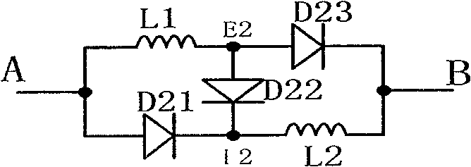
[0026] The step-up transmission ratio expansion circuit expands the number of stages n=2, and regards it as a two-port network AB, and the internal nodes are defined as E2 and F2 respectively (see figure 1 ), where node A is the inductor L 1 and diode D 21 Intersection of the anodes; node B is the inductor L 2 and diode D 23 Intersection of cathodes; internal node E2 is inductor L 1 and diode D 22 、D 23 The intersection point of the anode, the internal node F2 is the inductor L 2 and diode D21 、D 22 intersection point of the cathode.
Embodiment 2
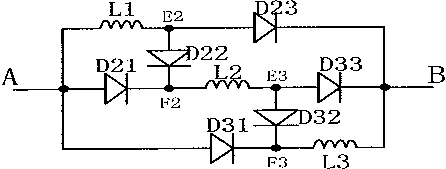
[0028] The step-up transmission ratio expansion circuit expands the number of stages n=3, and regards it as a two-port network AB, and the internal nodes are respectively defined as E2, E3 and F2, F3 (see figure 2 ), where node A is the inductor L 1 and diode D 21 、D 31 Intersection of the anodes; node B is the inductor L 3 and diode D 23 、D 33 Intersection of cathodes; internal node E2 is inductor L 1 and diode D 22 、D 23 The intersection point of the anode; E3 is the inductance L 2 and diode D 32 、D 33 Intersection of the anode; internal node F2 is the inductor L 2 and diode D 21 、D 22 The intersection point of the cathode; F3 is the inductance L 3 and diode D 31 、D 32 intersection point of the cathode.
Embodiment 3
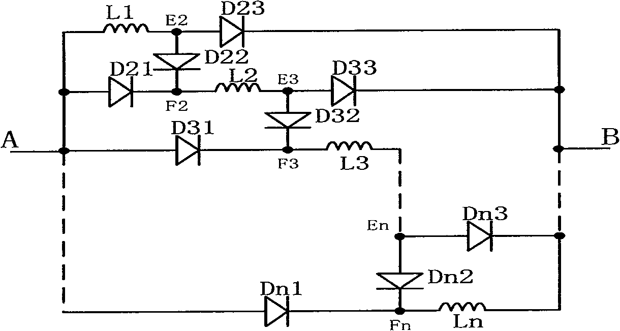
[0030] The expansion series of the step-up transmission ratio expansion circuit is n (2≤n≤500), and it is regarded as a two-port network AB, and the internal nodes are respectively defined as E2, E3...En and F2, F3...Fn (see image 3 ), where node A is the inductor L 1 and diode D x1 Intersection of the anodes; node B is the inductor L n and diode D x3 Intersection of cathodes; internal node E x is the inductance L x-1 and diode D x2 、D x3 Intersection of the anode, internal node F x is the inductance L x and diode D x1 and D x2 Intersection of cathodes (where x=2, 3...n).
PUM
 Abstract
Description
Claims
Application Information


