Display device

A display device and circuit board technology, applied in static indicators, cathode ray tube indicators, optics, etc., can solve problems such as complicated process, increased production cost, and increased size of display equipment

Inactive Publication Date: 2009-04-15
SAMSUNG DISPLAY CO LTD
View PDF3 Cites 0 Cited by
  • Summary
  • Abstract
  • Description
  • Claims
  • Application Information

AI Technical Summary

Problems solved by technology

These processes lead to an increase in the size of the display device due to the unoccupied space used for the connection
In addition, the process for mounting the integrated chip and for connecting the driver and auxiliary FPC is complicated and increases the production cost

Method used


Image

  • Display device
  • Display device
  • Display device

Examples


Embodiment Construction

[0021] Hereinafter, the present invention will be described more fully with reference to the accompanying drawings showing typical embodiments of the invention. However, the present invention can be embodied in many different forms and should not be limited to the scope as defined by the examples set forth herein.

[0022] In the drawings, the thickness of layers and regions are exaggerated for clarity. Like reference numerals refer to like parts throughout. It will be understood that when an element such as a layer, film, region, substrate or panel is referred to as being "on" another element, it can be directly on the other element or intervening elements may also be present. In contrast, when an element is referred to as being "directly on" another element, there are no intervening elements present.

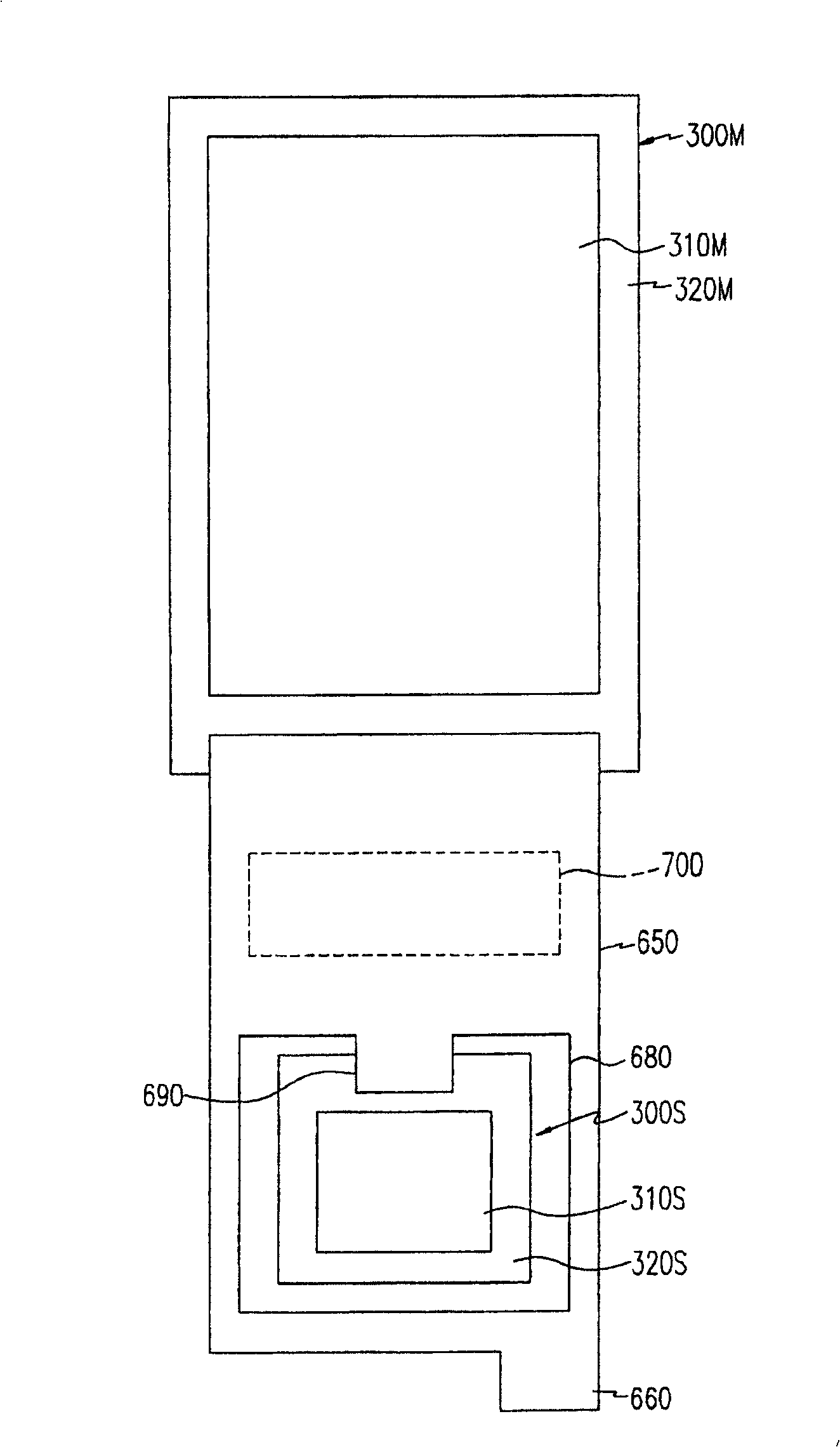
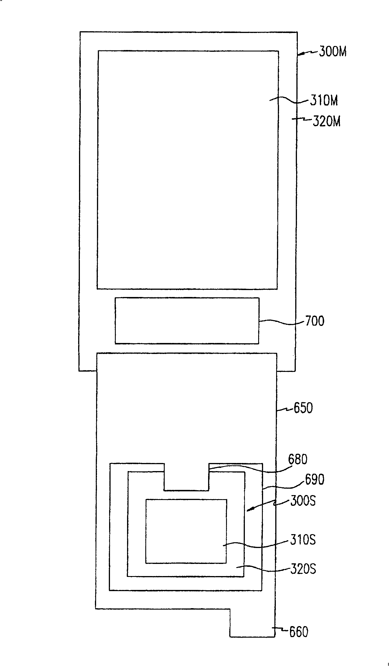
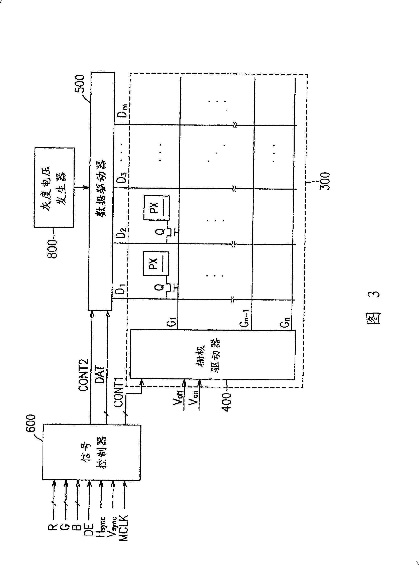
[0023] figure 1 is a schematic diagram of a display device according to an exemplary embodiment of the present invention. figure 2 is a schematic diagram of a display dev...


PUM


Abstract

A display device includes a circuit board provided with signal lines, a first and a second panel unit separately attached to the circuit board and each provided with pixels comprising switching elements, and a driving circuit chip mounted on the circuit board and driving the first and the second panel units.

Description

technical field [0001] The present invention relates to a display device. Background technique [0002] Recently, flat panel display devices have been widely developed, such as organic electroluminescent display (OLED) devices, plasma display panel (PDP) devices, and liquid crystal display (LCD) devices. Flat panel display devices are commonly used as a replacement for bulky and bulky cathode ray tube (CRT) display devices. [0003] The PDP device displays characters or images using plasma generated by gas discharge, and the OLED device displays characters or images using electroluminescent properties of specific organic or polymer molecules. The LCD device displays desired images by adjusting the transmittance of light passing through the liquid crystal layer by applying an electric field to a liquid crystal layer disposed between two panels and adjusting the strength of the electric field. [0004] As a particular type of display devices described above, dual display dev...

Claims


Application Information

Patent Timeline
Patent Type & Authority Patents(China)
IPC IPC(8): G09G5/14G09G3/20G02F1/1345
CPCG02F1/133305G02F1/13452G02F1/13458G02F1/136286H05K2201/05
Inventor 孟昊奭朱胜镛金喆镐朴基灿金哲民朴泰炯文国哲金一坤金治宇尹晋赫
Owner SAMSUNG DISPLAY CO LTD
Why Eureka
Try Eureka