Memory interface, memory arrangement and method of controlling memory access
What is AI technical title?
AI technical title is built by PatSnap AI team. It summarizes the technical point description of the patent document.
A memory interface and memory technology, applied in static memory, memory system, digital memory information, etc., can solve the problem of impossible memory area size balance, and achieve the effect of avoiding unauthorized access
Inactive Publication Date: 2009-07-29
NXP BV
View PDF4 Cites 0 Cited by
Summary
Abstract
Description
Claims
Application Information
AI Technical Summary
This helps you quickly interpret patents by identifying the three key elements:
Problems solved by technology
Method used
Benefits of technology
Problems solved by technology
[0005] The disadvantage found so far is that a separate memory interface must be designed for each product with a different memory configuration
Likewise, it is almost impossible to equalize the size of the memory area
Method used
Image
Click on the blue label to locate the original text in one second.
Reading with bidirectional positioning of images and text.
Examples
Embodiment Construction
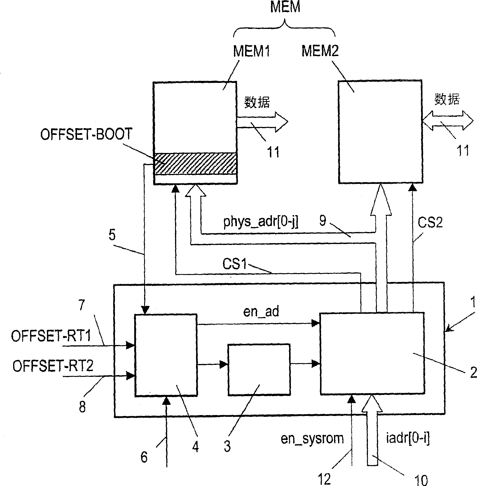
[0019] figure 2 is a block circuit diagram of an embodiment of a memory arrangement and a memory interface 1 according to the present invention, by which the above described in figure 1 The logical and physical partitioning of the memory is shown in the memory setup and memory interface 1. The memory arrangement comprises a program and / or data memory MEM comprising figure 1There are two memory modules MEM1 and MEM2, for example, the memory module MEM1 is in the form of a write-once ROM, while the memory module MEM2 is in the form of a rewritable EEPROM or flash memory. Individual memory locations in the memory modules MEM1 and MEM2 can be accessed via the physical address bus 9 . Their data (shown as “data”) can be read out via the data bus 11 , and also read in in the case of the rewritable memory module MEM2 . It should be mentioned that for the purposes of the present invention it does not matter whether the logical or physical division of the memory MEM is organized in...
PUM
Abstract
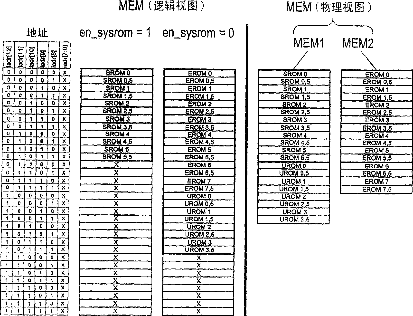
Disclosed is a kind of memory interface (1), is used for controlling to be divided into a plurality of memory areas (SROM0, ..., SROM5.5, EROM0, ..., EROM7.5, UROM0, ..., UROM3.5 ) program and / or data memory (MEM) access. The memory interface (1) includes: an address calculation device (2), which uses the offset value (OFFSET_BOOT, OFFSET_RT1, OFFSET_RT2) to perform a logical operation on the logical storage address (iadr[0-i]), and converts the logical storage address (iadr[0-i]) translates to a physical storage address (phys_adr[0-j]), where the offset value is assigned to a given memory area (SROM0, ..., SROM5.5, EROM0, ..., EROM7.5, UROM0, ..., UROM3.5), and are stored in the volatile offset memory (3). At least one offset value (OFFSET_BOOT) is read from a preset address in the program and / or data memory (MEM).
Description
technical field [0001] The invention relates to a memory interface for controlling access to a program and / or data memory divided into a plurality of memory areas, said memory interface comprising address calculation means for Shift values to perform logical operations on logical storage addresses, converting logical storage addresses to physical storage addresses. [0002] The invention also relates to a memory arrangement with a memory interface according to the invention. Finally, the invention also relates to a method of controlling access to a program and / or data memory divided into a plurality of memory areas, wherein the memory interface performs a logical memory The logical operation of the address converts the logical storage address into a physical storage address. Background technique [0003] Program and data memories having logically and physically distinct areas are well known in the art. Therefore, if figure 1 As shown in the left-hand part of , there is...
Claims
Application Information
Patent Timeline
Application Date:The date an application was filed.
Publication Date:The date a patent or application was officially published.
First Publication Date:The earliest publication date of a patent with the same application number.
Issue Date:Publication date of the patent grant document.
PCT Entry Date:The Entry date of PCT National Phase.
Estimated Expiry Date:The statutory expiry date of a patent right according to the Patent Law, and it is the longest term of protection that the patent right can achieve without the termination of the patent right due to other reasons(Term extension factor has been taken into account ).
Invalid Date:Actual expiry date is based on effective date or publication date of legal transaction data of invalid patent.

