Method for manufacturing substrate with emergent points

A manufacturing method and technology of bumps, which are applied in the field of manufacturing substrates with bumps, can solve problems such as difficult bumps, inability to install circuit components at the same time, and inability to select the height of bumps 108, etc., to achieve reliable electrical connection and manufacturing process The effect of simplicity and high reliability

Inactive Publication Date: 2009-07-29
ELEMENT DENSHI
View PDF5 Cites 0 Cited by
  • Summary
  • Abstract
  • Description
  • Claims
  • Application Information

AI Technical Summary

Problems solved by technology

[0008] Since bumps 108 are formed by solder, the height of bumps 108 cannot be selected
In addition, it is difficult to form a bump height of 100 μm or more by solder
[0009] In addition, since solder balls are placed and reflowed to form solder bumps 108, it is difficult to form the height of the bumps with high precision.
[0010] Since bumps are formed by soldering, solder paste is used on the mounting substrate and cannot be mounted simultaneously with other circuit components

Method used


Image

  • Method for manufacturing substrate with emergent points
  • Method for manufacturing substrate with emergent points
  • Method for manufacturing substrate with emergent points

Examples


Embodiment Construction

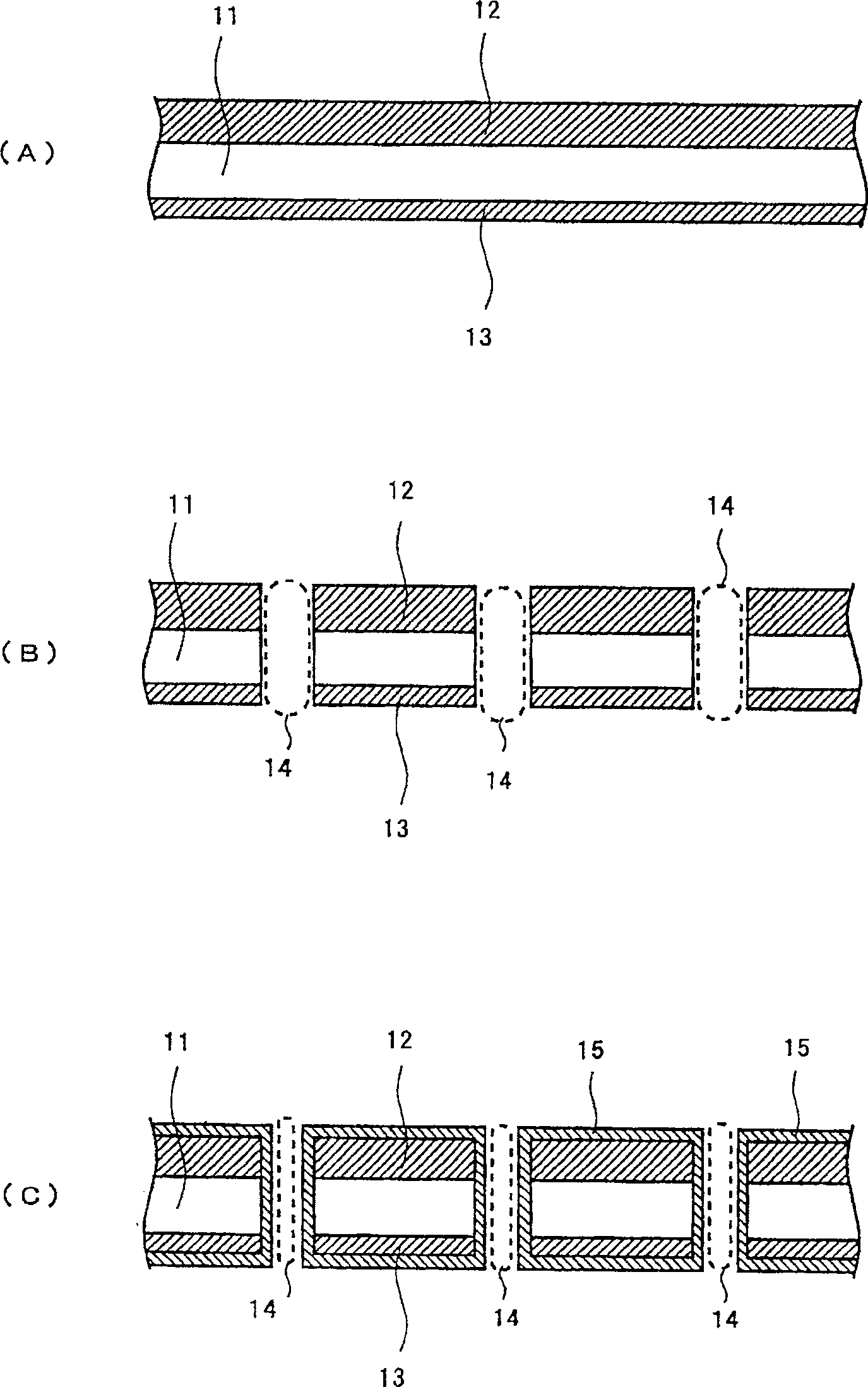
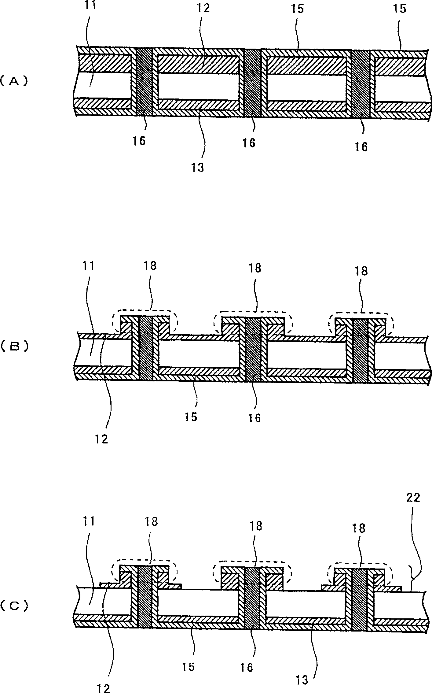
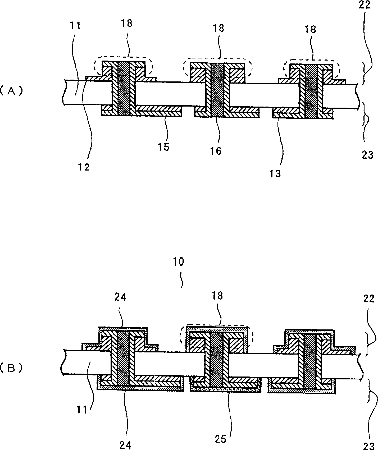
[0048] refer to Figure 1 ~ Figure 3 The method of manufacturing the circuit board of this embodiment will be described.

[0049] First, refer to figure 1 (A), the substrate 11 with the first conductive foil 12 pasted on the top and the second conductive foil 13 pasted on the bottom is prepared.

[0050] As the substrate 11, a glass epoxy substrate or a glass polyimide substrate is preferably used, but a fluorine substrate, a glass PPO substrate, a ceramic substrate, etc. may also be used depending on circumstances. In addition, flexible boards, films, and the like can also be used. In this embodiment, a glass epoxy substrate having a thickness of approximately 200 μm is used.

[0051] As the first conductive foil 12 and the second conductive foil 13, any metal that can be etched may be used. In this form, metal foil made of copper is used. Furthermore, copper foil having a film thickness of about 175 μm is used for the first conductive foil 12 . This film thickness is ...


PUM


Abstract

PROBLEM TO BE SOLVED: To provide a manufacturing method for a substrate with a bump capable of forming the high bump and capable of easily controlling the height of the bump.SOLUTION: The substrate is prepared in which a first conductive foil 12 is stuck on a top face first and a second conductive foil 13 is stuck on an underside, and a through-hole 14 is formed. The first conductive foil 12 and the second conductive foil 13 are connected electrically through the through-hole 14, and the through-hole 14 is filled with fillers 16. A conductive path extending from a bump 18 is formed by forming the bump 18 by etching the first conductive foil 12, and etching the first conductive foil 12 excepting a place where the bump 18 is formed. Accordingly, the height of the bump 18 can be controlled by controlling the thickness of the first conductive foil 12.

Description

technical field [0001] The present invention relates to a method of manufacturing a substrate with bumps that can form high bumps and can easily select the bump height. Background technique [0002] refer to Figure 7 A method for forming conventional solder bumps will be described. [0003] First, refer to Figure 7 (A), the first conductive pattern 102 is formed on the upper surface of the substrate 101, and the circuit substrate 100 is formed by forming the second conductive pattern 103 on the lower surface. [0004] refer to Figure 7 (B), the semiconductor element 104 is placed on the first conductive pattern 102 , and the first conductive pattern 102 and the semiconductor element 104 are electrically connected using the thin metal wire 105 . Further, the upper surface of the substrate 101 is sealed with a sealing resin 106 so as to cover the semiconductor element 104 and the thin metal wires 105 . [0005] refer to Figure 7 (C), patterning the resist 107 to expose d...

Claims


Application Information

Patent Timeline
Patent Type & Authority Patents(China)
IPC IPC(8): H01L21/48
CPCH01L2924/15311H01L2224/73265H01L2224/48227H01L2224/32225H01L24/73H01L2924/14
Inventor 成田悟郎
Owner ELEMENT DENSHI
Why Eureka
Try Eureka