A device and method for improving detection precision of oxidated layer thickness

A technology of oxide layer thickness and detection accuracy, which is applied in the field of wafer oxide layer thickness detection, can solve the problems of oxide layer thickness thinning, inaccurate measurement, and influence of wafer thickness control, and achieve the effect of stable thickness and precise process control

Inactive Publication Date: 2009-10-07
SEMICON MFG INT (SHANGHAI) CORP +1
View PDF3 Cites 1 Cited by
  • Summary
  • Abstract
  • Description
  • Claims
  • Application Information

AI Technical Summary

Problems solved by technology

[0004] The disadvantage of this method is that when the wafer boat is full of wafers, the upper surface of the control wafers in the middle and lower parts of the furnace tube will face the back of the wafer. For some special process products, different films on the back of the wafer will face The thickness of the control sheet has different effects
For example, for a 0.18 micron process wafer, the back of the wafer is a layer of silicon nitride film (Si 3 N 4 ), because the silicon nitride film has a repelling effect on oxygen, so when the chip is placed on the top of the control chip, the growth rate of silicon dioxide on the control chip will slow down, and the thickness of the oxide layer on the control chip will also become thinner, resulting in measurement imprecise

Method used


Image

  • A device and method for improving detection precision of oxidated layer thickness

Examples


Embodiment Construction

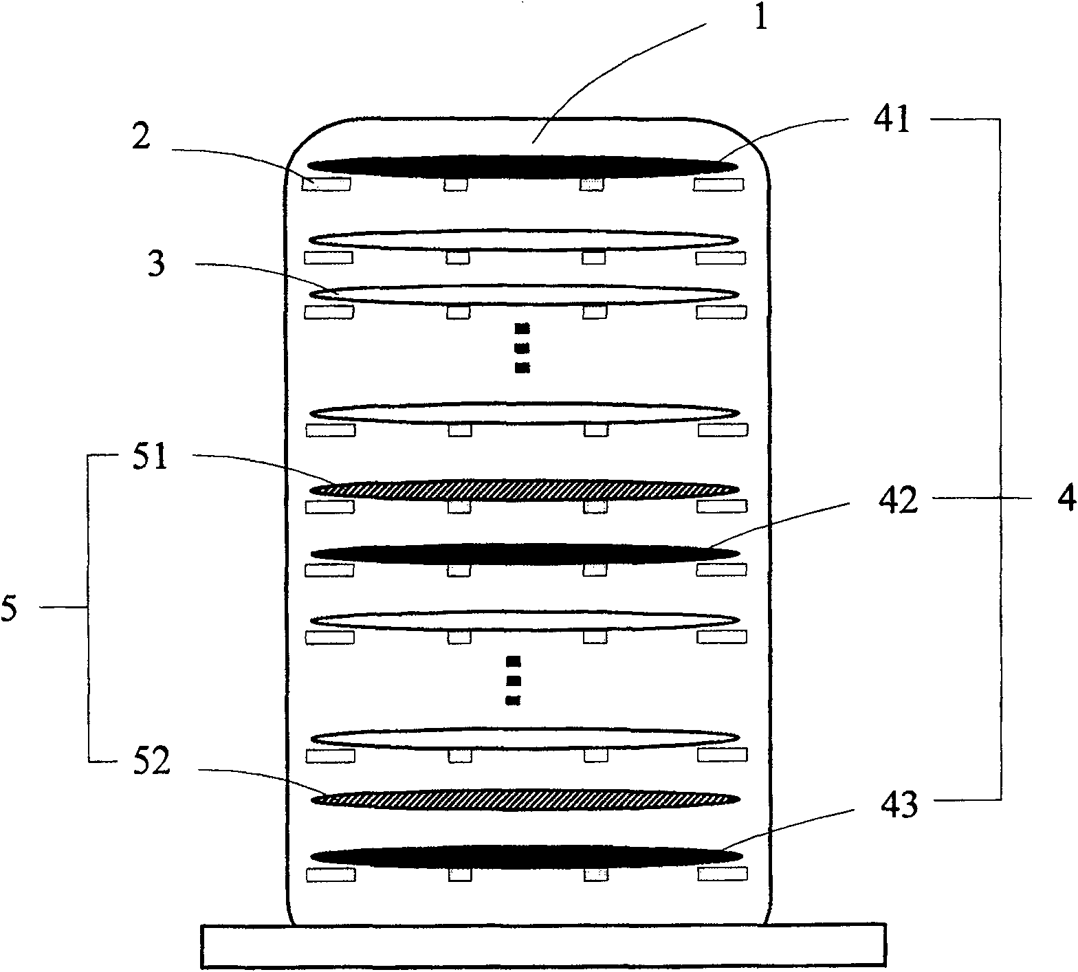
[0011] like figure 1 As shown, the present invention relates to the device that improves the detection accuracy of oxide layer thickness and comprises a furnace tube 1, a crystal boat 2, several wafers 3, three control sheets 4 (41,42,43) and two blocking sheets 5 (51 , 52).

[0012] see figure 1 , the wafer boat 2 is used to carry several wafers 3 , and the wafers 3 are arranged horizontally in the wafer boat 2 . The upper and lower surfaces of the three control sheets 4 and the two blocking sheets 5 are silicon oxide (SiO 2 ), the first control sheet 41 is located at the top of the wafer boat 2 , the second control sheet 42 is located at the middle of the wafer boat 2 , and the third control sheet 43 is located at the bottom of the wafer boat 2 .

[0013] At normal temperature, the machine (not shown) for loading the wafer 3 is set by the computer to reserve three vacancies for the upper, middle and lower wafer boat 2 for the control sheet 4, and the second control sheet ...


PUM


Abstract

The device for improving the detection accuracy of oxide layer thickness in the present invention includes a furnace tube, a crystal boat, several wafers and three control sheets placed on the top, middle and bottom of the crystal boat, and the wafers and control sheets are arranged and placed on the crystal boat. A blocking sheet is also placed above the control sheets located in the middle and bottom of the crystal boat. In addition, the present invention also provides a method for improving the detection accuracy of the thickness of the oxide layer, which includes loading several wafers and three control plates into the wafer boat, and placing a blocking plate respectively above the control plates at the middle and bottom of the wafer boat, and then Lift the crystal boat into the furnace tube for oxidation. In the present invention, the baffle arranged above the control plate can effectively prevent the thin film on the lower surface of the wafer from affecting the growth of the oxide layer of the control plate during the oxidation process, so that the thickness of the oxide layer on the three control plates is more stable, and can truly and accurately reflect the thickness of the entire furnace. The condition of the tube, which is conducive to more precise process control of the oxidation of the entire furnace tube.

Description

technical field [0001] The invention relates to a semiconductor manufacturing process, in particular to detection of the thickness of an oxide layer of a wafer. Background technique [0002] Since the wafer surface has a high affinity for oxygen molecules, it is easy to form an oxide layer when the wafer surface is exposed to an oxygen-containing atmosphere. At present, the commonly used method is to place the wafer in the furnace tube, then raise it to an appropriate temperature, and feed oxygen or water vapor and other oxygen-containing gases to grow a layer on the wafer, which has good adhesion to silicon materials and is insulating. The best silica. [0003] It is usually necessary to detect the thickness of the gate oxide layer to judge whether the process is up to standard. At present, the detection method for the thickness of the gate oxide layer in the furnace tube area is: place a control chip on the top, middle and bottom of the crystal boat, and measure the thic...

Claims


Application Information

Patent Timeline
Patent Type & Authority Patents(China)
IPC IPC(8): H01L21/66
Inventor 翟志刚
Owner SEMICON MFG INT (SHANGHAI) CORP
Why Eureka
Try Eureka