Photoresist coating device and its method

A technology of photoresist and spraying device, which can be applied to devices for coating liquids on surfaces, coatings, photo-engraving process coating equipment, etc., and can solve problems such as inconvenience, no adjustment, and unfavorable production efficiency.

Inactive Publication Date: 2009-11-18
SEMICON MFG INT (SHANGHAI) CORP +1
View PDF5 Cites 0 Cited by
  • Summary
  • Abstract
  • Description
  • Claims
  • Application Information

AI Technical Summary

Problems solved by technology

The photoresist coating device in the prior art does not provide means to adjust the concentricity between the photoresist nozzle and the wafer and the height of the photoresist nozzle from the wafer. It can only be adjusted visually by engineers, and the results are very inaccurate. Adjustments are required before lithography, which is very inconvenient and not conducive to improving production efficiency

Method used


Image

  • Photoresist coating device and its method
  • Photoresist coating device and its method
  • Photoresist coating device and its method

Examples


Embodiment Construction

[0070] The specific implementation manners of the present invention will be described in detail below in conjunction with the accompanying drawings.

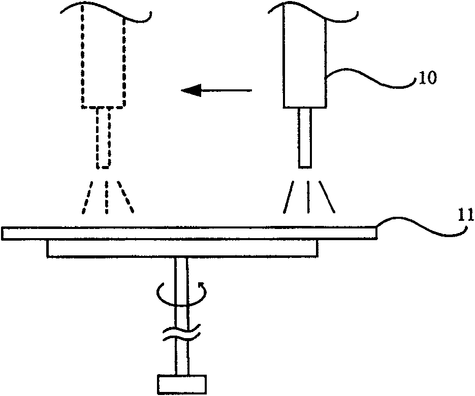
[0071] The photoresist spraying device of the present invention plays a key role in spraying the photoresist on the wafer surface in order to form a uniform photoresist film on the wafer surface during the photolithography process. The invention utilizes the dummy nozzle to calibrate the concentricity of the nozzle and the wafer and the height of the nozzle from the wafer surface. In a preferred embodiment, the scale axis in the dummy nozzle is extended by 5±0.1 mm from the lower end surface of the housing, that is, the height of the nozzle from the wafer surface is adjusted to 5±0.1 mm. The implementation process and essential content of the present invention are described with preferred embodiments.

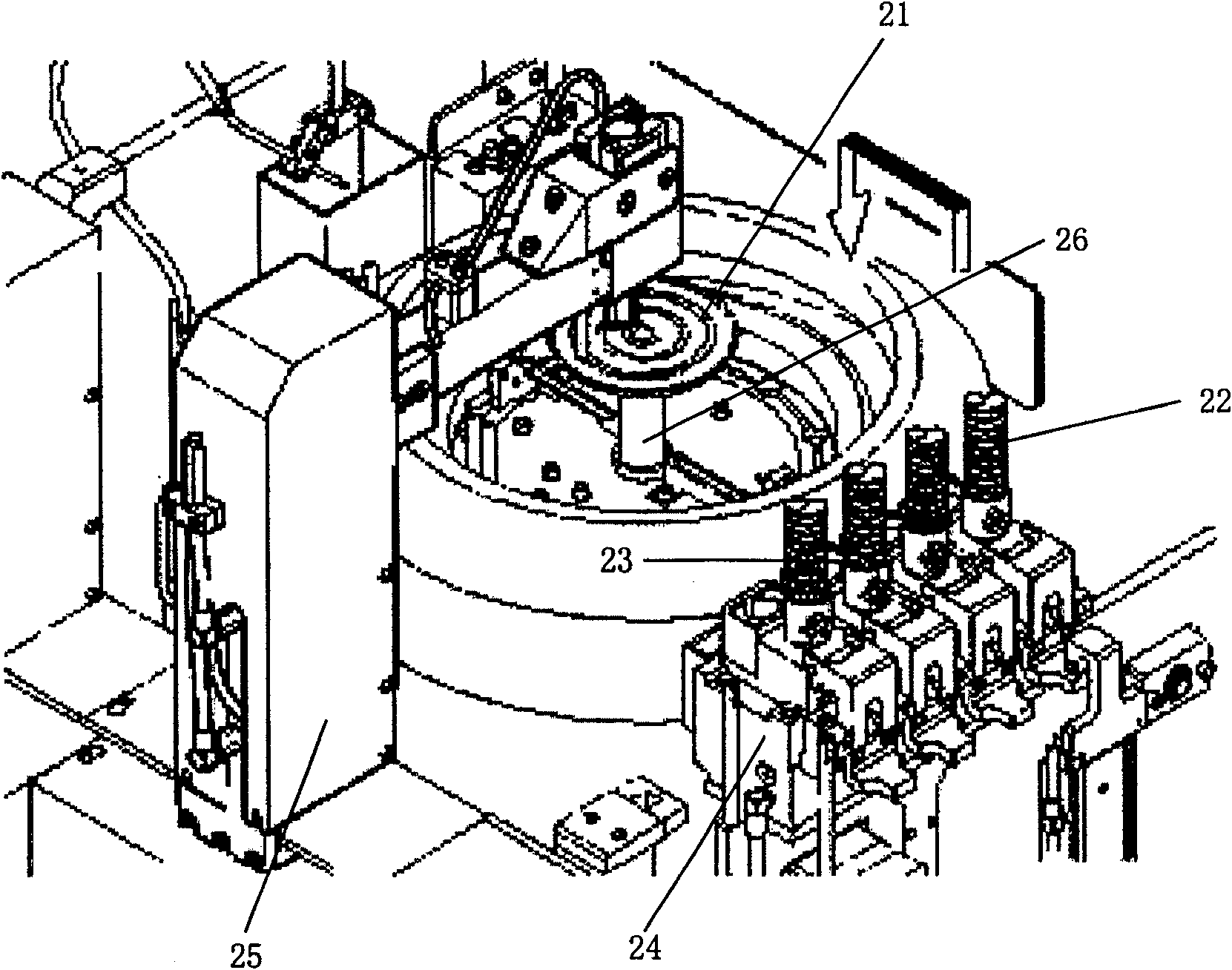
[0072] figure 2 It is a structural schematic diagram of the photoresist spraying device of the present invention. Such as ...


PUM


Abstract

The invention discloses a photoresist spraying device, which comprises a nozzle for spraying photoresist; a nozzle slot for placing at least one photoresist nozzle; a nozzle for grabbing the photoresist nozzle and driving the nozzle to move and lift Grabbing arm; a wafer carrier that carries the wafer that needs to be sprayed with photoresist; a rotating mechanism that drives the wafer carrier to rotate; a pseudo nozzle placed in the nozzle slot to calibrate the concentricity and height of the nozzle and the wafer surface; control the nozzle grip a control system for moving the arm and memorizing the position at which the nozzle grabbing arm grabs the nozzle; and a photoresist supply system for supplying photoresist to the nozzle. The present invention also provides a kind of method of spraying photoresist correspondingly, comprise the concentricity and height of nozzle grabbing dummy nozzle calibration nozzle and wafer surface; Wafer surface; photoresist is sprayed onto the wafer surface.

Description

technical field [0001] The invention relates to a photoresist coating device used in the photolithography process, in particular to a photoresist coating device in which the position between the photoresist nozzle and the wafer can be precisely positioned during the photolithography process Devices and methods. Background technique [0002] The photolithography process is one of the most frequently used and most critical technologies in chip manufacturing technology. For semiconductor components, optoelectronic devices, etc., it is necessary to use the photolithography process to transfer the mask patterns of the basic components and circuits of the required components to On the photoresist pattern on the surface of the substrate, such as a wafer or a glass substrate. Usually, the basic process of photolithography includes three steps: glue coating, exposure and development. The purpose of the coating process is to create a thin, uniform, and defect-free photoresist film o...

Claims


Application Information

Patent Timeline
Patent Type & Authority Patents(China)
IPC IPC(8): G03F7/16B05C11/08
Inventor 陈林炯胡晓明张峻铭
Owner SEMICON MFG INT (SHANGHAI) CORP
Why Eureka
Try Eureka