Device and method for sticking substrate

A technology for manufacturing devices and manufacturing methods, which is applied in the field of liquid crystal display devices, and can solve the problems of lower yield, light leakage in light-shielding parts, uneven display, etc., and achieve the effect of easy maintenance and reduced configuration area

Inactive Publication Date: 2009-12-02
FUJITSU LTD
View PDF4 Cites 0 Cited by
  • Summary
  • Abstract
  • Description
  • Claims
  • Application Information

AI Technical Summary

Problems solved by technology

This shift in the position of the substrate causes light leakage in the light-shielding part and display defects such as uneven display, and is a major cause of yield reduction.

Method used


Image

  • Device and method for sticking substrate
  • Device and method for sticking substrate
  • Device and method for sticking substrate

Examples


Embodiment Construction

[0028] (first embodiment)

[0029] Below, refer to Figure 1 to Figure 4 , the first embodiment of the present invention will be described.

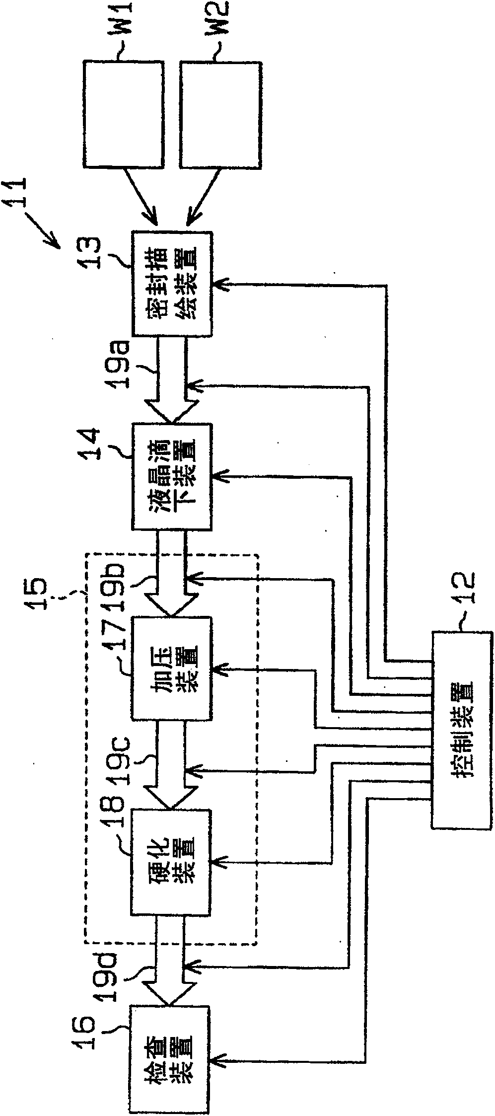
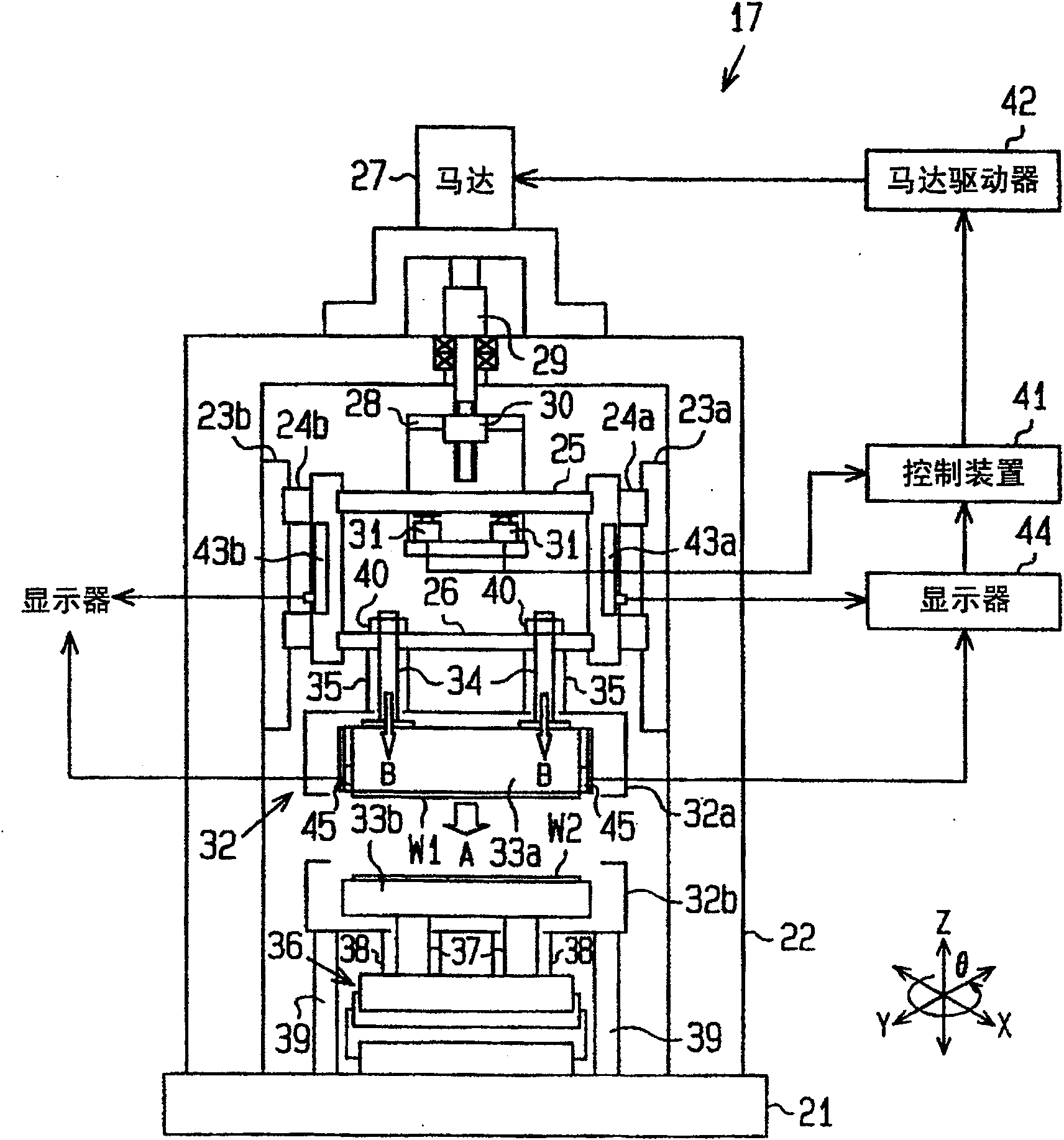
[0030] figure 1 This is a schematic structural diagram of a bonded substrate manufacturing apparatus that implements the steps of injecting and bonding liquid crystal in the liquid crystal cell process in the manufacturing process of a liquid crystal display device.

[0031] The bonded substrate manufacturing apparatus 11 seals liquid crystal between the supplied two types of substrates W1 and W2 to manufacture a liquid crystal display substrate. The liquid crystal display panel manufactured in this embodiment is, for example, an active matrix type liquid crystal display panel. The first substrate W1 is a color filter substrate (CF substrate) on which a color filter and a light-shielding film are formed, and the second substrate W2 is a color filter substrate (CF substrate) on which a color filter is formed. Array substrates (TFT subs...


PUM


Abstract

PURPOSE: An apparatus and a method for fabricating a bonded substrate are provided to avoid side slip of the substrate by means of repulsive force of process pressure generated when bonding two substrates together. CONSTITUTION: In an apparatus for fabricating a bonded substrate, a first substrate and a second substrate are adsorbed into a first retention plate(61) and a second retention plate(62) arranged to face each other in a chamber, by using either pressure difference adsorption or electrostatic adsorption, and are bonded together by approaching them to each other. Either the first retention plate or the second retention plate is provided with a frictional resistor that retains the first and second substrates by frictional resistance, thereby failing to cause an error in the position between the substrates when bonding them to each other.

Description

technical field [0001] The present invention relates to a bonded substrate manufacturing apparatus and a bonded substrate manufacturing method. More specifically, the present invention relates to a substrate ( Appropriate bonded substrate manufacturing apparatus and bonded substrate manufacturing method for use in panels). Background technique [0002] In recent years, flat display panels such as LCDs have been increased in size and weight (thinned), and at the same time, further cost reductions have been demanded. For this reason, it is required to improve yield and productivity in an apparatus for manufacturing a panel by bonding two substrates together. [0003] Liquid crystal display panels are, for example, array substrates (TFT substrates) on which a plurality of TFTs (thin film transistors) are formed in a matrix, and color filter substrates (CF substrates) on which color filters (red, green, blue) and light-shielding films are formed. ) are arranged facing each oth...

Claims


Application Information

Patent Timeline
Patent Type & Authority Patents(China)
IPC IPC(8): G02F1/1339G02F1/136G02F1/13G02F1/133H01L21/00
CPCA44C1/00A44C25/00
Inventor 桥诘幸司宫岛良政伊藤彰悦
Owner FUJITSU LTD
Why Eureka
Try Eureka