Circuit board and manufacturing method thereof

A technology of circuit boards and substrates, which is applied in the manufacture of printed circuits, circuits, printed circuits, etc., can solve problems such as inability to observe, and achieve the effects of improving productivity, improving efficiency, and suppressing whitening

Inactive Publication Date: 2009-12-16
SHINKO
View PDF4 Cites 0 Cited by
  • Summary
  • Abstract
  • Description
  • Claims
  • Application Information

AI Technical Summary

Problems solved by technology

However, when the opening is formed by press working, the part without the wiring pattern around the opening is affected by the press working. Figure 13 In the part shown, a whitish-looking whitened area 6 with a size of about 0.3mm is partially newly generated
[0007] This whitened area 6 can be observed from the surface of the circuit board, so in subsequent steps such as wire bonding, there may be problems in image recognition, etc., and it is necessary to eliminate the occurrence of the whited area or make it very small, or make it become unable to observe

Method used


Image

  • Circuit board and manufacturing method thereof
  • Circuit board and manufacturing method thereof
  • Circuit board and manufacturing method thereof

Examples


Embodiment

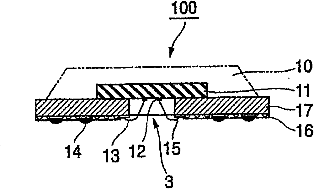
[0074] Using a 0.18mm-thick glass substrate epoxy resin copper-clad laminate with a 0.02mm-thick copper layer on one side, after laminating a photoresist on the copper layer, exposure and development are performed using a photomask To etch the copper layer to form wiring patterns and dummy patterns of various shapes and sizes.

[0075] Next, solder resist is applied, exposure and development are performed using a given mask, and Ni plating of 10 μm and Au plating of 0.7 μm are performed on the surface of the copper layer of the dummy patterns and wiring patterns that appear. Then, press working is performed using a die to form openings.

[0076] In addition, dummy patterns and wiring patterns in such as Figure 10 As shown, after forming a pattern that is electrically integrally connected on the portion that becomes the opening, press processing is used, such as figure 2 Electrical continuity is cut off as shown.

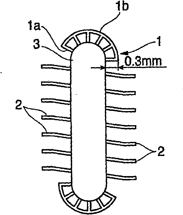
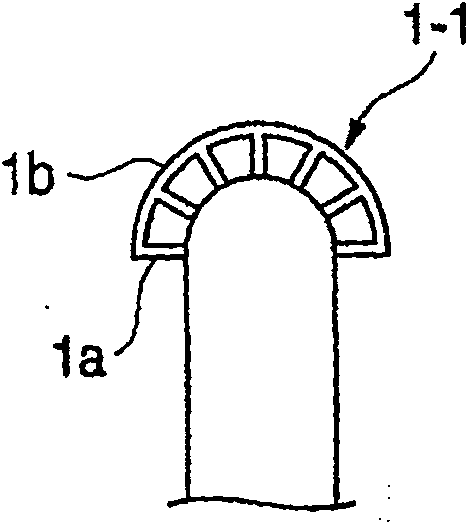
[0077] In the arc portion of the opening, from Figure 3 ...


PUM

PropertyMeasurementUnit
widthaaaaaaaaaa
angleaaaaaaaaaa
thicknessaaaaaaaaaa

Abstract

The present invention provides a circuit board in which generation of a white-blushed mark which is partially produced at a blank portion having no wiring pattern at a rim of an opening portion is suppressed when forming the opening portion by punching, and a manufacturing method thereof in the circuit board in which a portion where a wiring pattern is dense and the blank portion having no wiring pattern are present at a rim of a central part of the circuit board. There is provided a circuit board having an opening portion formed at the center of the circuit board by punching, the circuit board having a structure where a dummy electrode pattern connected with a rim of the opening portion is provided besides a wiring pattern which is connected with the opening portion at the rim of the opening portion and used for wire bonding. It is preferable to provide the dummy electrode pattern having a size satisfying S / d>=0.33, where S is an area of the dummy electrode pattern and d is a sum total of lengths of sides where the dummy electrode pattern is connected with the rim of the opening portion.

Description

technical field [0001] The present invention relates to a circuit board on which a semiconductor element is mounted, that is, a circuit board having an opening in the center for connecting the semiconductor element and the circuit board with bonding wires, and a method for manufacturing the same. Background technique [0002] Generally, when semiconductor elements are mounted on electronic equipment, semiconductor elements are mounted on circuit boards in advance, and the circuit boards on which semiconductor elements are mounted are assembled into electronic equipment to improve the efficiency of mounting work. At this time, the electrodes of the semiconductor element and the terminals on the circuit board are connected with bonding wires. In order to shorten the length of the bonding wire, an opening is provided in the center of the circuit board, and electrodes of small semiconductor elements are connected to terminals of circuit wiring around the opening with bonding wir...

Claims


Application Information

Patent Timeline
Patent Type & Authority Patents(China)
IPC IPC(8): H01L23/498H01L21/48H05K1/02H05K3/00
CPCH01L2924/15311H05K2203/175H05K3/005H01L2224/4824H01L2924/01078H05K3/242H01L2924/01079H01L24/48H01L23/49838H05K2201/09781H05K2203/049H01L2924/181H01L2924/00014Y10T29/49162H01L2924/00012H01L2224/45099H01L2224/45015H01L2924/207H01L23/48H01L23/12
Inventor 野原贵誉丈
Owner SHINKO
Why Eureka
Try Eureka