Delay locked loop circuit and method for provding delay locked loop clock of synchronous memory device

A delay-locked loop and memory technology, applied in the field of DLL circuits, can solve the problems of difficult data transmission and different phases.

Inactive Publication Date: 2010-03-10
SK HYNIX INC
View PDF3 Cites 0 Cited by
  • Summary
  • Abstract
  • Description
  • Claims
  • Application Information

AI Technical Summary

Problems solved by technology

As a result, it is difficult to accurately transfer data to / receive data from DRAM because the phase of the external clock signal is different from that of the DLL clock signal DLL_CLK of the DLL circuit

Method used


Image

  • Delay locked loop circuit and method for provding delay locked loop clock of synchronous memory device
  • Delay locked loop circuit and method for provding delay locked loop clock of synchronous memory device
  • Delay locked loop circuit and method for provding delay locked loop clock of synchronous memory device

Examples


Embodiment Construction

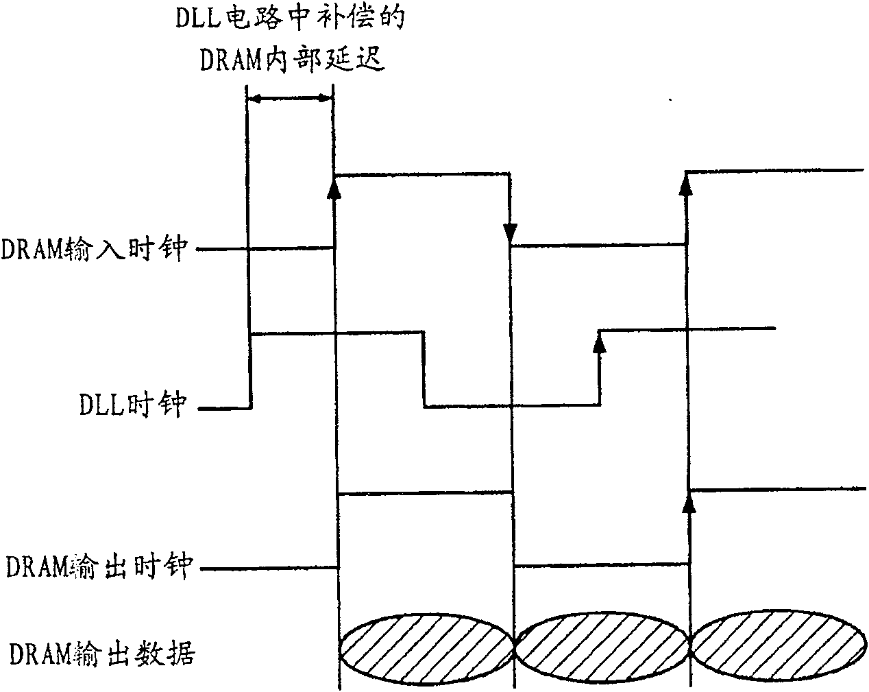
[0052] A delay locked loop (DLL) circuit according to an exemplary embodiment of the present invention will be described in detail with reference to the accompanying drawings.

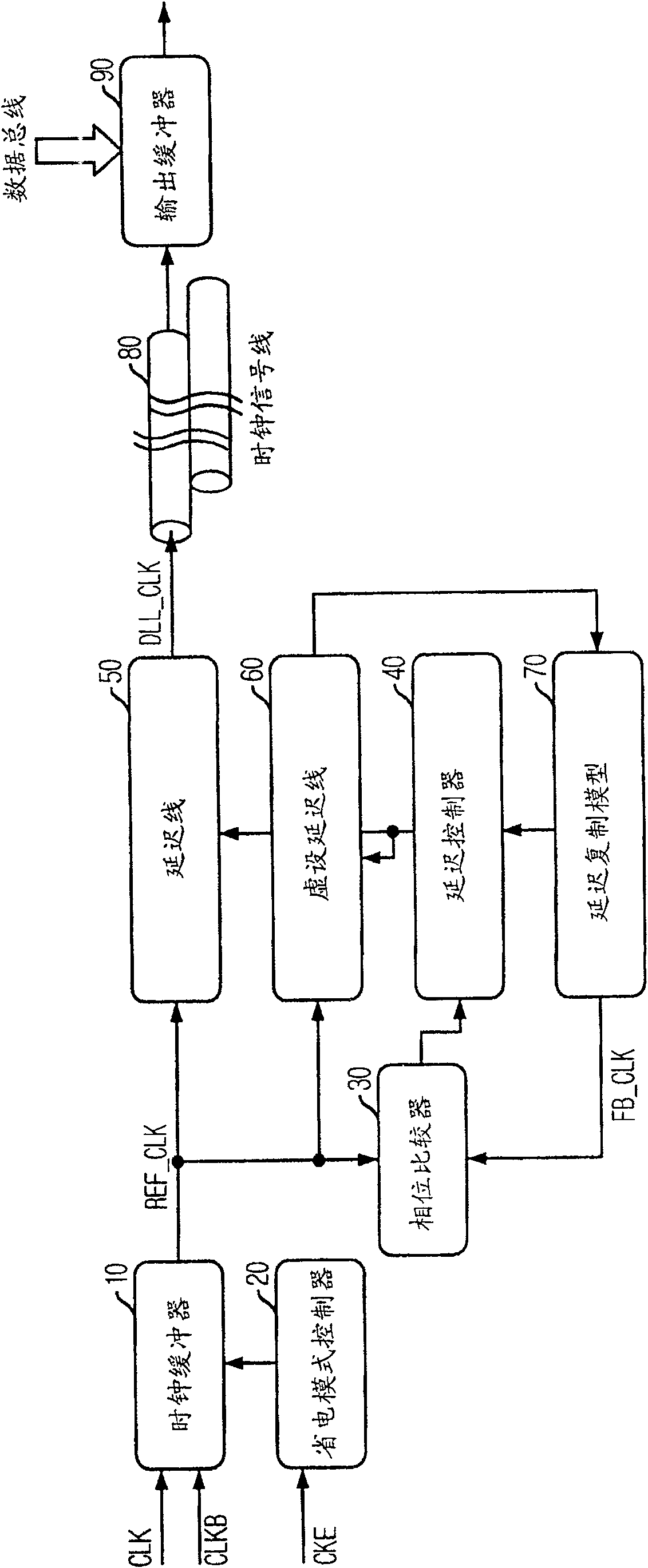
[0053] Figure 4 is a block diagram of a DLL circuit according to an embodiment of the present invention.

[0054] The DLL circuit 600 includes a power saving mode controller 100 , a first clock buffer 200 and a second clock buffer 300 , a clock selection unit 400 and a phase update unit 500 .

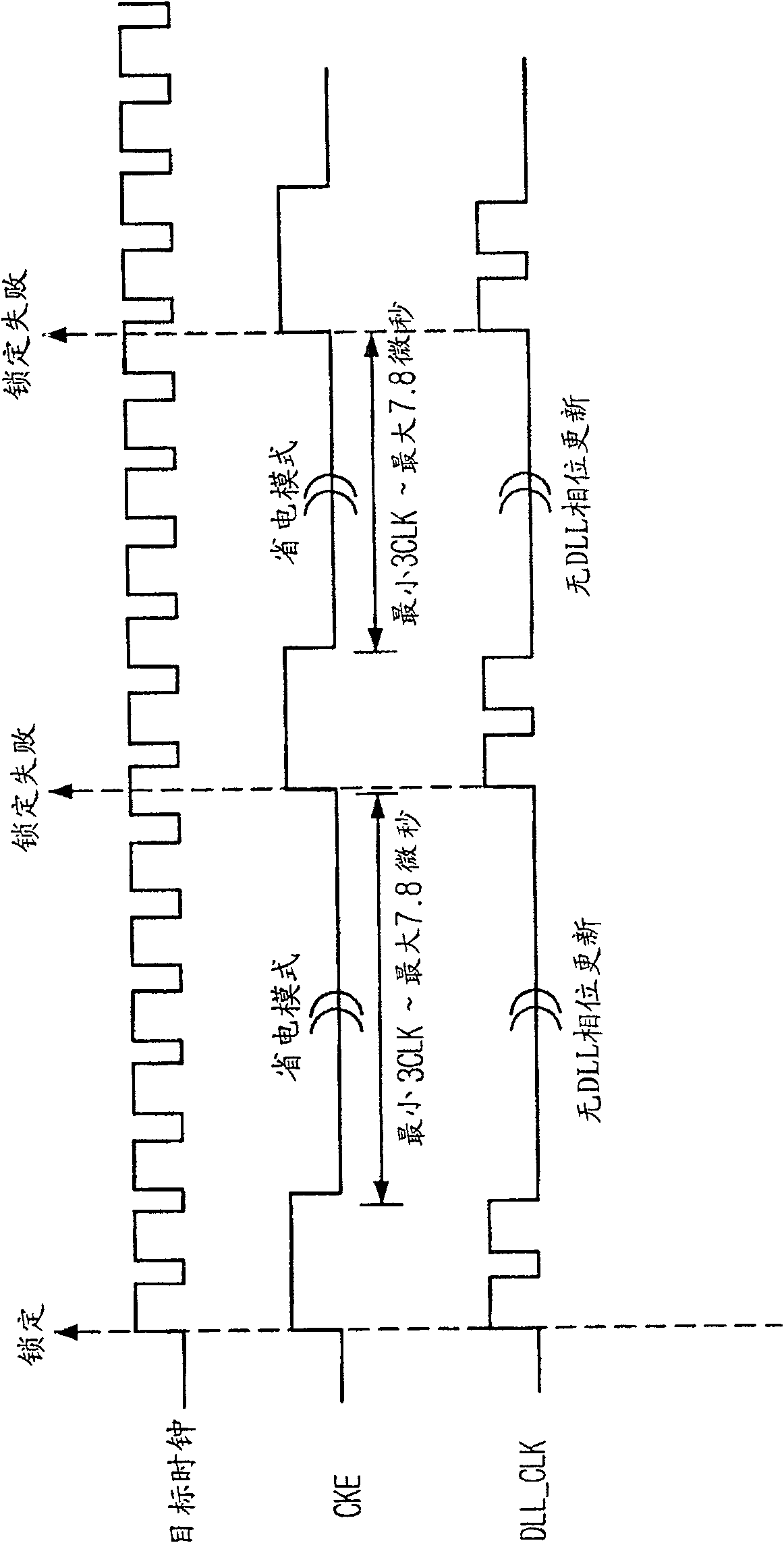
[0055] The power saving mode controller 100 generates a power saving mode control signal CTRL which determines initiation or termination of the power saving mode in response to the clock enable signal CKE.

[0056] The first clock buffer 200 receives and buffers the external clock signal CLK and the external clock bar signal CLKB in response to the power saving mode control signal CTRL, thereby outputting the buffered signal as the first internal clock signal ICLK_NM. .

[0057] The second clock buffer 300 r...


PUM


Abstract

A synchronous memory device having a normal mode and a power down mode includes a power down mode controller for generating a power down mode control signal in response to a clock enable signal, thereby determining onset or termination of a power down mode. A clock buffering unit buffers an external clock signal in response to the power down mode control signal and outputs first and second internal clock signals. A clock selection unit selects one of the first and second internal clock signals based on the power down mode control signal to output the selected signal as an intermediate output clock signal. A phase update unit performs a phase update operation by using the intermediate output clock signal to output a delay locked loop (DLL) clock signal, the first internal clock signal differing in frequency from the second internal clock signal.

Description

technical field [0001] The present invention relates to a delay locked loop (DLL) circuit of a synchronous DRAM, and more particularly, the present invention relates to a DLL circuit performing stable operation in a power saving mode for low power operation of a semiconductor device. Background technique [0002] A synchronous semiconductor memory device such as a double data rate synchronous DRAM (DDR SDRAM) performs data transfer with an external device using an internal clock signal synchronously locked to an external clock signal input from an external device such as a memory controller. In order to transmit data stably, the data should be precisely positioned at the edge or center of the clock by compensating for delay time inevitably caused by a time difference between data transmission of each component and data loaded into the bus. [0003] The clock synchronization circuit used to compensate the delay time is a phase-locked loop (PLL) or a delay-locked loop (DLL). ...

Claims


Application Information

Patent Timeline
Patent Type & Authority Patents(China)
IPC IPC(8): G11C7/10
CPCG11C7/222G11C7/225G11C11/4076G11C2207/2227H03L7/0812
Inventor 崔勋
Owner SK HYNIX INC
Why Eureka
Try Eureka