Optoelectronic device, element driving device and electronic equipment

A technology of electro-optical devices and electro-optical components, which is applied in the field of component drive devices and component substrates, and can solve problems such as crystal defects, pixel circuit difficulties, and disordered characteristics

Inactive Publication Date: 2007-08-08
INTELLECTUAL KEYSTONE TECH LLC
View PDF1 Cites 10 Cited by
  • Summary
  • Abstract
  • Description
  • Claims
  • Application Information

AI Technical Summary

Problems solved by technology

However, in low-temperature polysilicon, disordered characteristics tend to occur during recrystallization, and crystal defects may also occur
Therefore, in a display device using a thin film transistor composed of low-temperature polysilicon, it is extremely difficult to make the electrical characteristics of the pixel circuit uniform throughout the pixel.
In particular, as the number of pixels is increased for displaying high-definition images and large screens, the possibility of disorderly differences in the characteristics of each pixel circuit becomes higher, and the problem of display quality degradation becomes more significant.

Method used


Image

  • Optoelectronic device, element driving device and electronic equipment
  • Optoelectronic device, element driving device and electronic equipment
  • Optoelectronic device, element driving device and electronic equipment

Examples


Embodiment Construction

[0123] Hereinafter, embodiments of the present invention will be described with reference to the accompanying drawings. The following forms are only one form of the present invention, and do not limit the present invention, and can be changed arbitrarily within the scope of the present invention. In addition, in each of the drawings shown below, the size and ratio of each component are appropriately different from the actual size and ratio in order to make each component a recognizable size on the drawing.

[0124]

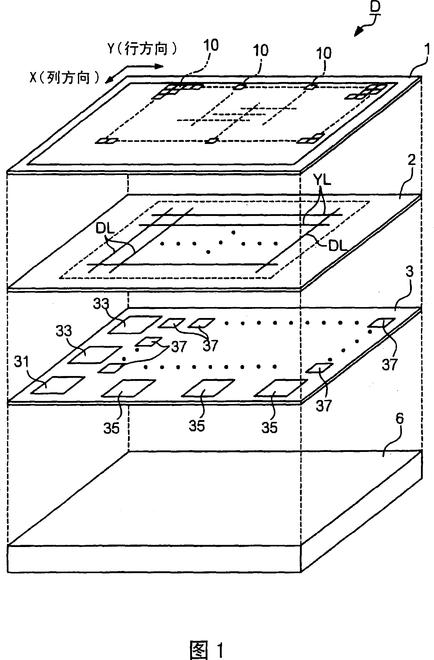
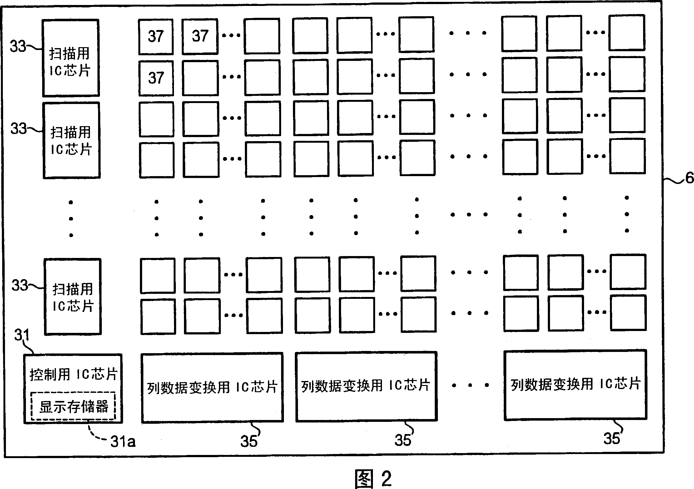
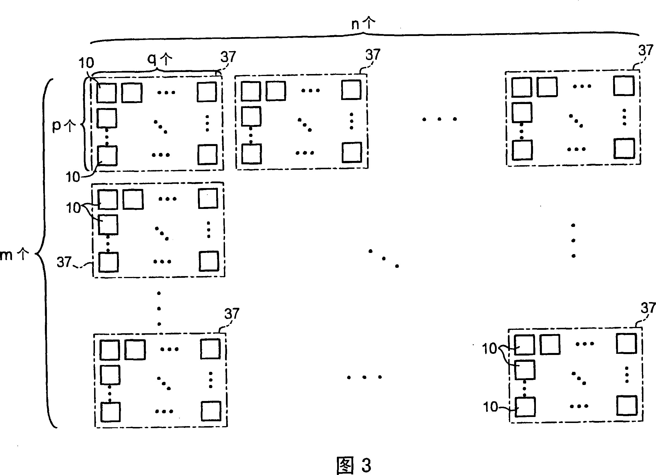
[0125] First, as a device for displaying an image, an embodiment applicable to the electro-optical device of the present invention will be described. FIG. 1 is a perspective view showing the structure of an electro-optical device according to an embodiment of the present invention. As shown in the figure, the electro-optical device D has a support substrate 6 , an organic EL layer 1 , a wiring formation layer 2 , and an electronic component layer 3 . The support...


PUM

PropertyMeasurementUnit
lengthaaaaaaaaaa
thicknessaaaaaaaaaa
thicknessaaaaaaaaaa

Abstract

An electro-optic device comprises a plurality of electronic components; a plurality of IC chips used for driving a plurality of circuits of the electronic components; a control circuit for choosing respectively more than one unit circuit for driving the electronic components and meanwhile carrying out the driving operation; and a choosing circuit for choosing respectively more than one IC chip and meanwhile making the control circuit which has chosen the IC chip carry out the choosing and controlling.

Description

[0001] This application is an application number "03801726.1", the title of the invention is "electro-optical device and its manufacturing method, component drive device and its manufacturing method, component substrate and electronic equipment", and its filing date is May 29, 2003. case application. technical field [0002] The present invention relates to an element driving device for driving a plurality of driven elements and a manufacturing method thereof, and more particularly to an electro-optical device using an electro-optical element for converting an electric effect as a driven element and a manufacturing method thereof. into light effect. The present invention relates to an element substrate suitable for an element driving device and an electro-optical device, and electronic equipment including the electro-optical device and the element driving device. Background technique [0003] As display devices for various electronic devices such as mobile phones and PDAs (...

Claims


Application Information

Patent Timeline
Patent Type & Authority Applications(China)
IPC IPC(8): G02F1/1345G02F1/133G09G3/36
Inventor 今村阳一
Owner INTELLECTUAL KEYSTONE TECH LLC
Why Eureka
Try Eureka