Plasma display device
A display device and plasma technology, applied in identification devices, instruments, cooling/ventilation/heating transformation, etc., can solve the problems of reduced grounding ability, weak fixing ability, weak bonding ability, etc., to improve the electromagnetic wave cut-off rate and easy fixing Effect
- Summary
- Abstract
- Description
- Claims
- Application Information
AI Technical Summary
Problems solved by technology
Method used
Image


Examples
Embodiment Construction
[0043] Hereinafter, the present invention will be specifically described with reference to the drawings and examples.
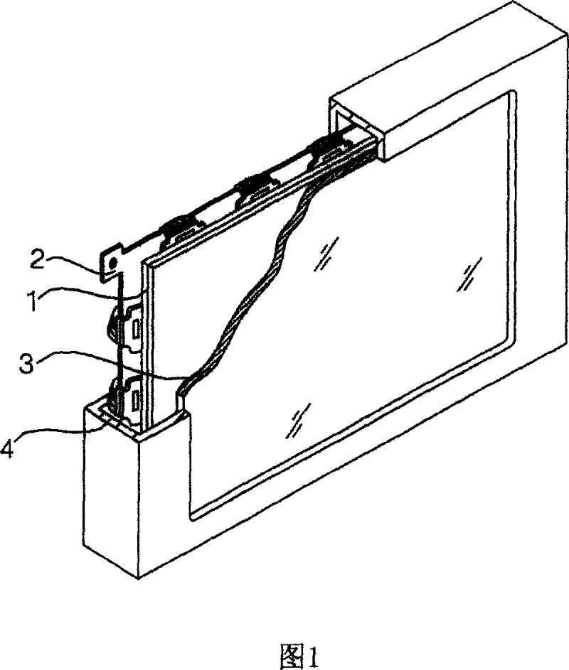
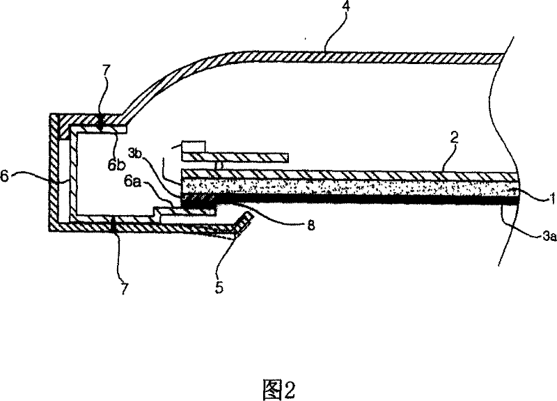
[0044] 3 is a schematic view showing the structure of the ground clip of the plasma display device of the present invention, and FIG. 4 is a schematic view showing a first example of the plasma display device of the present invention.
[0045] The plasma display device of the present invention includes a substrate 10, a filter 20 for shielding electromagnetic waves in the front of the substrate, a heat dissipation plate 30 fixed on the back of the substrate, and the filter, the substrate, and the heat dissipation plate are clamped to make the above-mentioned The filter 20, the above-mentioned substrate 10 and the above-mentioned heat sink 30 are simultaneously fixed on the ground clip 100 at the edge position of the above-mentioned substrate.
[0046] The above-mentioned substrate 10 is a component in which a front substrate on which a plurality of scan elect...
PUM
 Abstract
Description
Claims
Application Information
 - R&D
- Intellectual Property
- Life Sciences
- Materials
- Tech Scout
- Unparalleled Data Quality
- Higher Quality Content
- 60% Fewer Hallucinations
Browse by: Latest US Patents, China's latest patents, Technical Efficacy Thesaurus, Application Domain, Technology Topic, Popular Technical Reports.
© 2025 PatSnap. All rights reserved.Legal|Privacy policy|Modern Slavery Act Transparency Statement|Sitemap|About US| Contact US: help@patsnap.com