Pixel level multi-task architecture driving method and device using the method

A driving method and multi-tasking technology, applied to instruments, static indicators, etc., can solve the problems of increasing charging time, reducing the response speed of liquid crystal display, poor display quality of liquid crystal display, etc., and achieve the effect of increasing response speed

Inactive Publication Date: 2007-11-28
INNOLUX CORP
View PDF0 Cites 11 Cited by
  • Summary
  • Abstract
  • Description
  • Claims
  • Application Information

AI Technical Summary

Problems solved by technology

[0009] However, for scan lines coupled to the SL n Pixel B 1,n , which only scans the line SL n The first period T of the upper scan signal 1 is turned on to accept the data line DL 1 The data signal has not been pre-charged, which will reduce the response speed of the LCD screen display
[0010] In addition, due to the PLM structure, the time required for the pixel (especially pixel B) to be fully charged is longer than that of the non-PLM structure, so it may not be able to charge to the predetermined voltage level, resulting in poor display quality of the LCD display ; Or increase the charging time, which will also reduce the response speed of the LCD screen display

Method used


Image

  • Pixel level multi-task architecture driving method and device using the method
  • Pixel level multi-task architecture driving method and device using the method
  • Pixel level multi-task architecture driving method and device using the method

Examples


Embodiment Construction

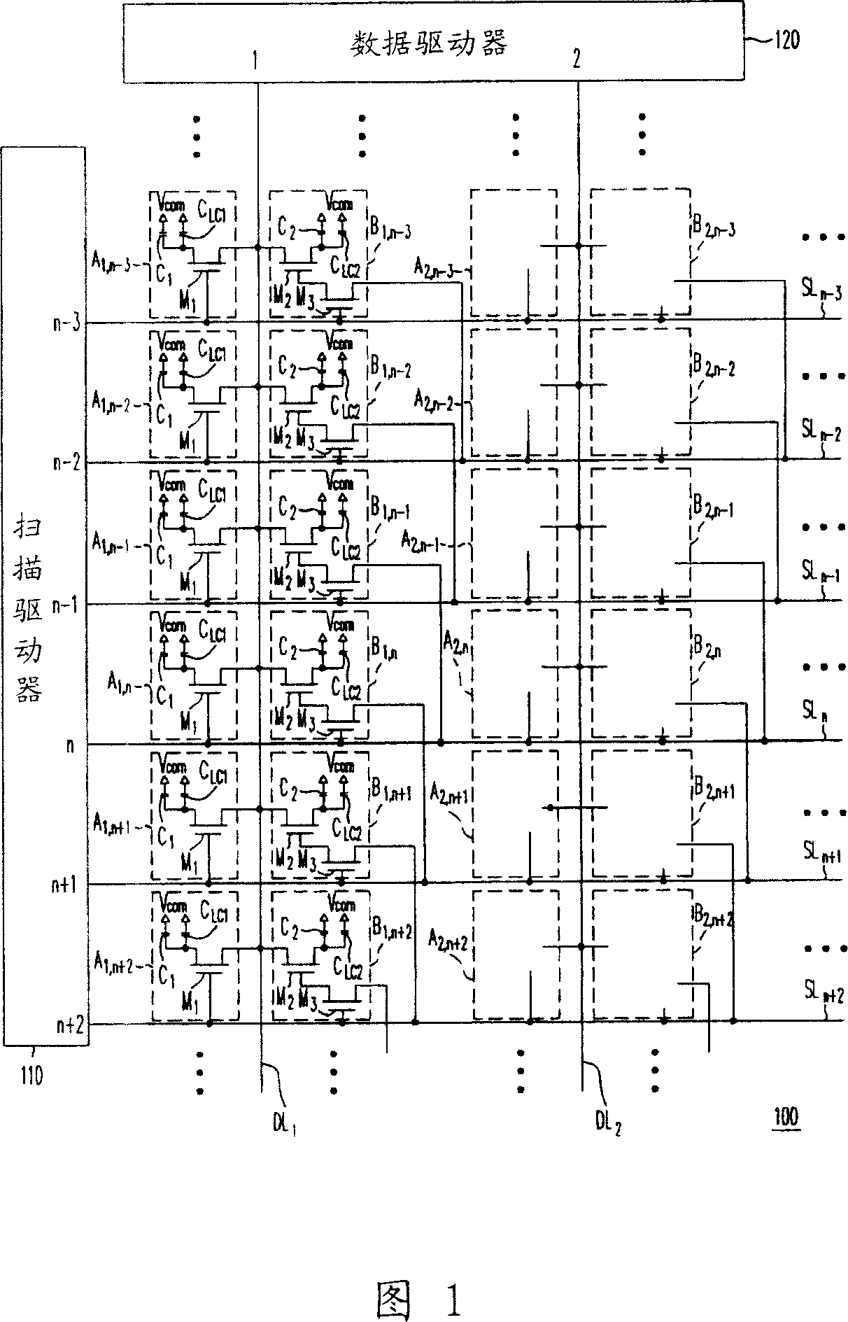
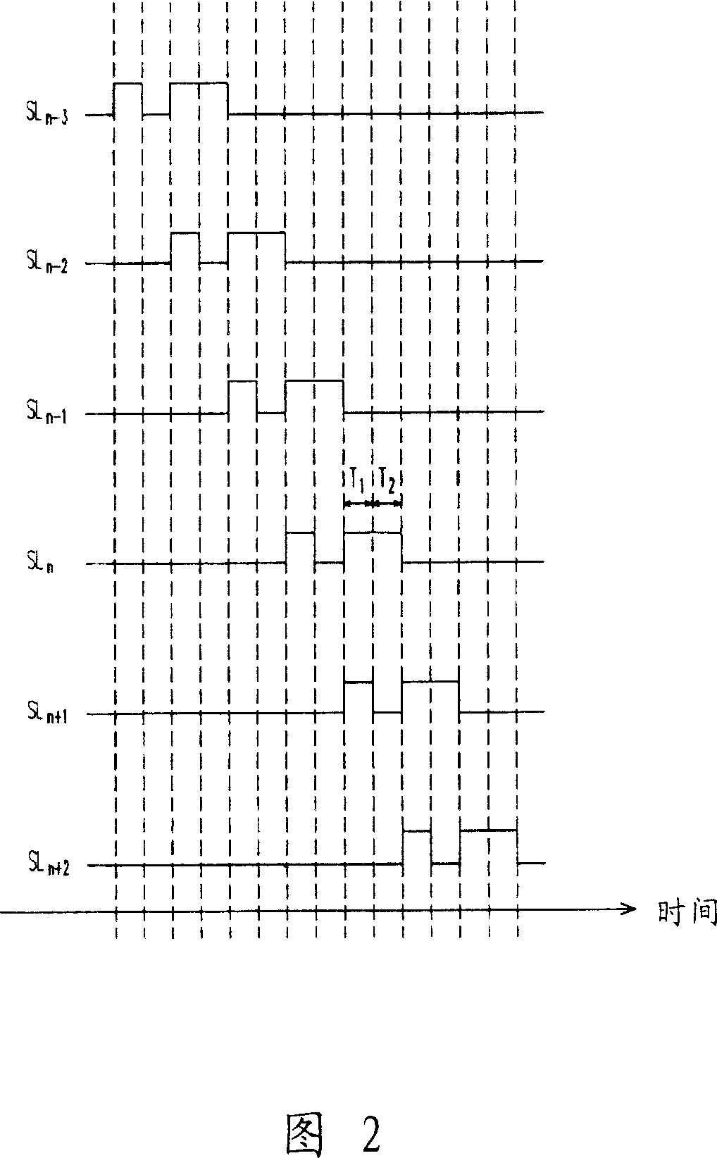
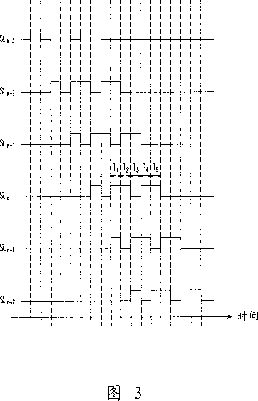
[0034] FIG. 3 shows a driving method according to a preferred embodiment of the present invention on the pixel level multiplexing (PLM) architecture shown in FIG. 1 , which shows a timing diagram of signals on each scanning line. Please refer to FIG. 1 first, the PLM architecture 100 includes a scan line SL driven by a scan driver 110 n-3 ~SL n+2 , the data line DL driven by the data driver 120 1 ~DL 2 , and "pixel A" and "pixel B" disposed on both sides of the data line, wherein n-3, n-1, . . . , n+2 are all positive integers.

[0035] Among them, "Pixel A" includes Pixel A 1,n-3 ~A 1,n+2 with A 2,n-3 ~A 2,n+2 Wait. For example, pixel A 1,n-3 that is coupled to the data line DL 1 with scanline SL n-3 The pixel A, or coupled to the data line DL 1 The n-3th pixel A of . while pixel A 2,n that is coupled to the data line DL 2 with scanline SL n The pixel A, or coupled to the data line DL 2 The nth pixel A of . Similarly, "Pixel B" includes Pixel B 1,n-3 ~B 1,n...


PUM


Abstract

The invention discloses a driving method of pixel level multi-task (PLM) frame with each dataline of PLM frame connecting two pixel A and pixel B at two ends of dataline, which comprises the following steps: transmitting the driving signal through scanning circuit sequently; precharging pixel B at jth pixel during charging the j-2nd pixel A; precharging pixel A at jth during charging the jth pixel B (j is more than 2, which is positive integral).

Description

technical field [0001] The present invention relates to a pixel level multiplexing (PLM) architecture, in particular to a driving method capable of precharging pixels in a pixel level multiplexing architecture and a device using the method . Background technique [0002] There are various types of flat panel displays (FPDs), such as liquid crystal displays (LCDs), organic electroluminescent displays (OLEDs), and plasma displays (PDPs). However, no matter what kind of flat panel display, the structure of the display panel is similar, that is, the substrate is provided with criss-cross scan lines and data lines, and each scan line is connected to the data line. One pixel is allocated at the line intersection. The pixels receive scan signals through the scan lines to determine whether they are enabled or turned on, and receive data signals through the data lines to display images when they are turned on. [0003] In order to reduce the cost, it is known that each data line i...

Claims


Application Information

Patent Timeline
Patent Type & Authority Applications(China)
IPC IPC(8): G09G3/20G09G3/36G02F1/133
Inventor 林丽年纪佳宏
Owner INNOLUX CORP
Why Eureka
Try Eureka