Production technology for high-precision fully resistance carbon film overlapping board

A production process and high-precision technology, applied in the direction containing printed electrical components, can solve the problems of increased manufacturing costs, low work efficiency, and product quality that cannot be further improved, so as to reduce manufacturing costs, meet production needs, and break through applications field effect

Active Publication Date: 2008-01-16
徐立军
View PDF0 Cites 14 Cited by
  • Summary
  • Abstract
  • Description
  • Claims
  • Application Information

AI Technical Summary

Problems solved by technology

Not only the work efficiency is low, the manufacturing cost is gre

Method used


Image

  • Production technology for high-precision fully resistance carbon film overlapping board

Examples


Embodiment 1

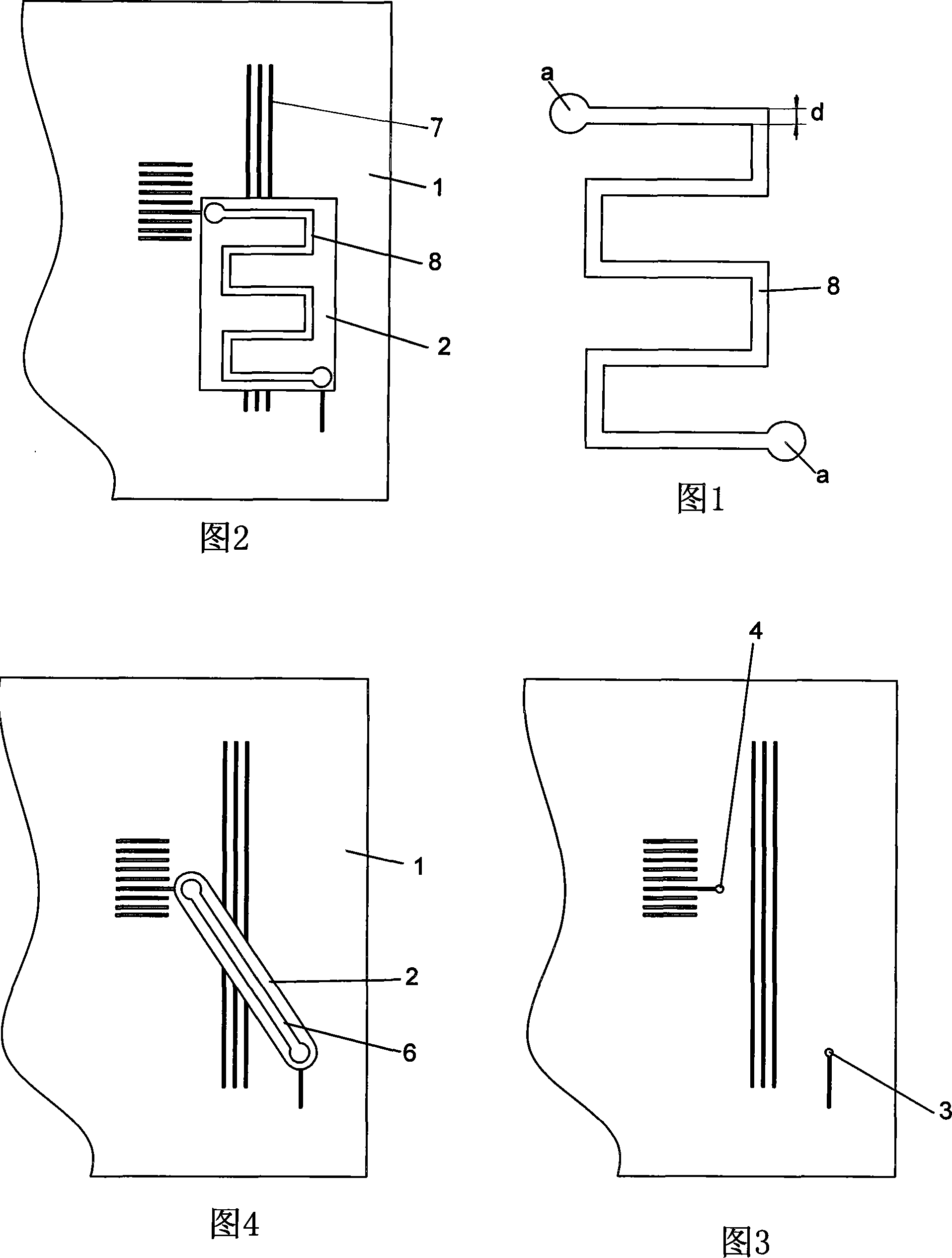
[0032] Embodiment 1: The user requires the resistance value of the bridge resistor to be 500±20%Ω.

[0033] According to the user's original design (see Figure 4), the carbon film resistor 6 has a length of 1.5cm, a width of 0.2cm, and is printed with fixed carbon oil of 25Ω / □ ("□" means square centimeter, and the thickness of the film is 25чm). According to the calculation formula provided by the present invention, in order to ensure that the resistance value of the resistor is within the range of 500 ± 20% Ω, the length of the carbon film resistor is changed in design, namely:

[0034] Length of carbon film resistor = resistance value of carbon film resistor × width of carbon film resistor ÷ resistance value of fixed carbon oil used = 500Ω×0.2cm÷25Ω=4cm.

[0035] After the length of the carbon film resistor is changed according to this length (the shape of the changed carbon film resistor 8 is shown in Figure 1), the actual resistance value is between 480 and 520Ω after batc...

Embodiment 2

[0036] Embodiment 2: The user requires the resistance value of the bridge resistor to be 300±20%Ω.

[0037] According to the user's original design, the carbon film resistor has a length of 2cm and a width of 0.3cm. It is printed with fixed carbon oil of 25Ω / □ ("□" means square centimeter, and the thickness of the film is 25чm). According to the calculation formula provided by the present invention, in order to ensure that the resistance value of the resistor is within the range of 300 ± 20% Ω, the length of the carbon film resistor is changed in design, namely:

[0038] Length of carbon film resistor = resistance value of carbon film resistor × width of carbon film resistor ÷ resistance value of fixed carbon oil used = 300Ω×0.3cm÷25Ω=3.6cm.

[0039] After the length of the carbon film resistor is changed according to this length (the shape of the changed carbon film resistor is shown in Figure 1), the actual resistance value is between 280 and 330Ω after batch tracking and me...

Embodiment 3

[0040] Embodiment 3: The user requires the resistance value of the bridge resistor to be 1000±20%Ω.

[0041] According to the user's original design, the carbon film resistor has a length of 2cm and a width of 0.15cm. It is printed with fixed carbon oil of 25Ω / □ ("□" means square centimeter, and the thickness of the film is 25чm). According to the calculation formula provided by the present invention, in order to ensure that the resistance value of the resistor is within the range of 1000 ± 20% Ω, the length of the carbon film resistor is changed in design, namely:

[0042] Length of carbon film resistor = resistance value of carbon film resistor × width of carbon film resistor ÷ resistance value of fixed carbon oil used = 1000Ω×0.15cm÷25Ω=6cm.

[0043] After the length of the carbon film resistor is changed according to this length (the shape of the changed carbon film resistor is shown in Figure 1), the actual resistance value is between 960 and 1050Ω after batch tracking an...


PUM

PropertyMeasurementUnit
Lengthaaaaaaaaaa
Widthaaaaaaaaaa
Thicknessaaaaaaaaaa

Abstract

The invention relates to a printing technology for high-resistance carbon film layer. The problem to be solved is that the provided technology can effectively realize resistance control on a high-resistance carbon film lamination, further to improve production efficiency and reduce production cost. The technical proposal is that the production technology for the high-precision whole-resistance carbon film laminated plate includes a production technology for a carbon film surface adhering plate in which a carbon film resistor is printed during printing process for the carbon film lamination. The printing process of the carbon film resistor is performed by following steps in sequence: firstly, determining proportion of the conductive carbon ink; and secondly, printing the conductive carbon ink on copper coil contact points at two ends of a resistor on the circuit board to form a carbon film resistor. The geometric shape of the carbon film resistor is determined by the following relationship: resistance of the carbon film resistor is equal to resistance of the formula of the carbon ink multiplied by length of the carbon film resistor and then divided by width of the carbon film resistor, in which the resistance of the carbon film resistor is determined by thickness of the carbon film resistor and the proportion of the conductive carbon ink, and width of the carbon film resistor is determined by thickness of the printed film.

Description

technical field [0001] The invention relates to a production process of a printed circuit board, in particular to a printing process of a high-resistance carbon film layer. Background technique [0002] A printed circuit is a conductive pattern that is printed on an insulating substrate according to a predetermined design, printed into a printed circuit board, printed components, or a combination of the two. The printed circuit board is a conductive pattern that provides electrical connections between components on an insulating substrate. Today's printed circuit boards used in digital audio and video home appliances, game consoles, etc. generally use single-sided (carbon film) boards and double-sided (carbon paste holed, silver paste holed, metal holed boards) boards. The traditional printed circuit board has only been used as a basic load-carrying circuit until now. [0003] The high-precision full-resistance carbon film laminate fully considers the resistance characteri...

Claims


Application Information

Patent Timeline
IPC IPC(8): H05K1/16
Inventor 徐立军
Owner 徐立军
Why Eureka
Try Eureka