Semiconductor element with U shaped drift region

一种半导体、漂移区的技术,应用在半导体器件、电固体器件、电气元件等方向,能够解决成本提高、工艺复杂性等问题,达到电流关断时间缩短、工艺简单、降低成本的效果

Inactive Publication Date: 2008-01-23
UNIV OF ELECTRONICS SCI & TECH OF CHINA
View PDF3 Cites 14 Cited by
  • Summary
  • Abstract
  • Description
  • Claims
  • Application Information

AI Technical Summary

Problems solved by technology

It goes without saying that this feature in the substrate leads to increased process complexity and cost

Method used


Image

  • Semiconductor element with U shaped drift region
  • Semiconductor element with U shaped drift region
  • Semiconductor element with U shaped drift region

Examples


Embodiment Construction

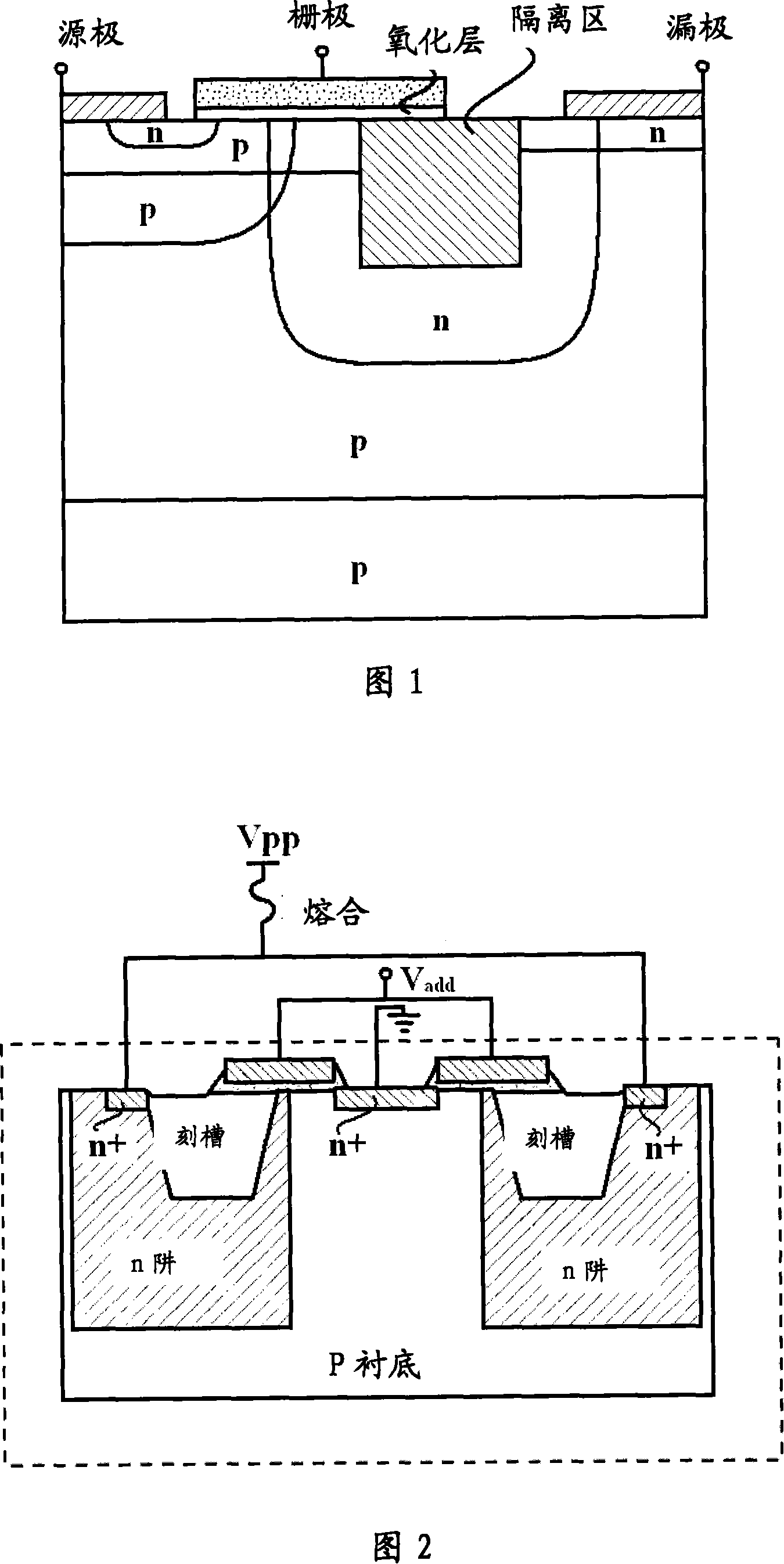
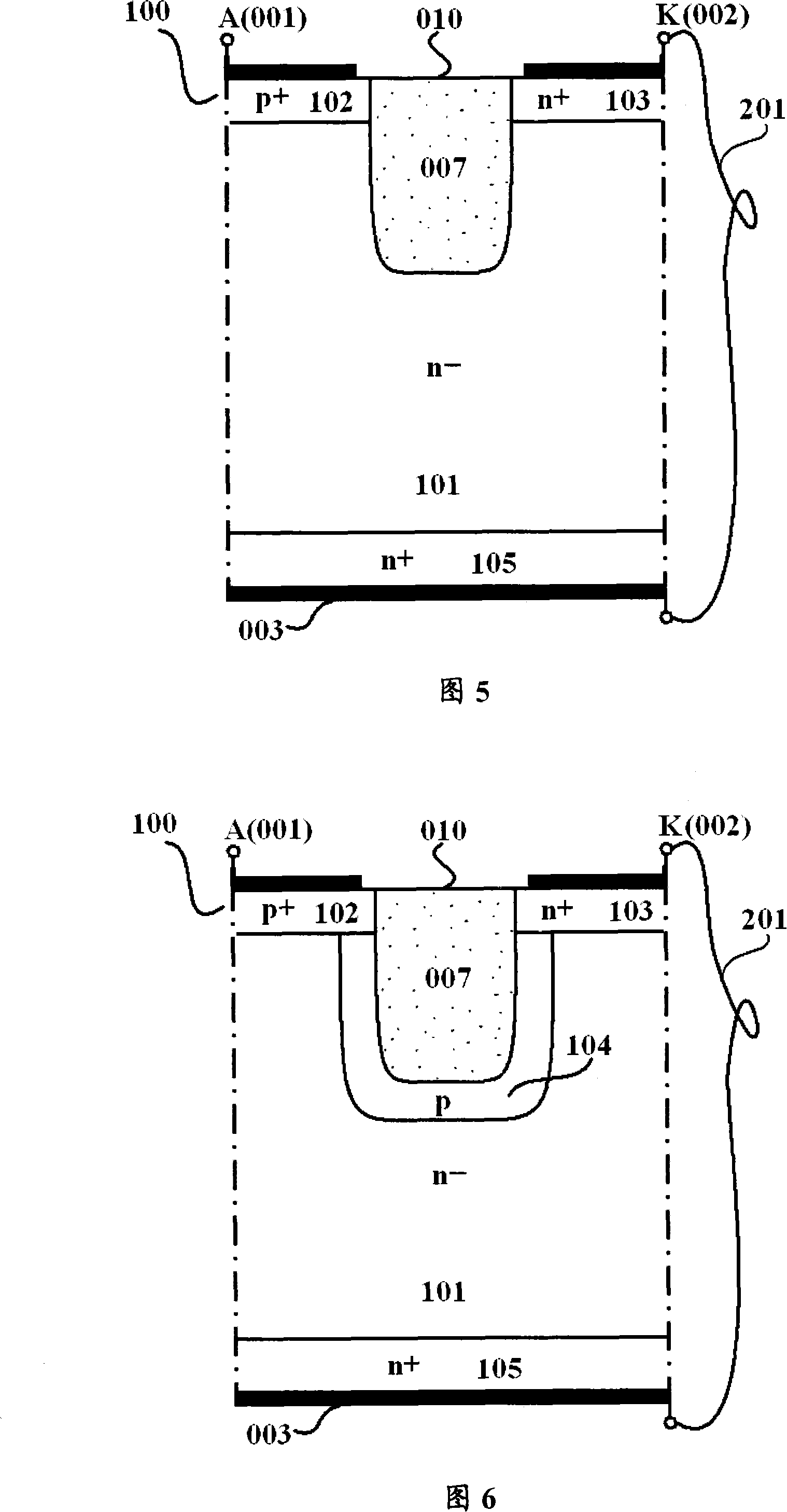
[0060] The withstand voltage situation of the drift region of the present invention is firstly explained with a p-n diode, because actually the withstand voltage situation of the drift region of various devices can be regarded as the situation of a p-n junction under reverse bias voltage. FIG. 5 shows a schematic cross-sectional view of the structure of a unit 100 of a device proposed by the present invention. Dotted lines in the figure indicate boundaries between one cell and another. n in the figure - Area 101 is a drift area, which is in the shape of a "U". Between the two sides of the "U" is a slot 010 filled with an insulator 007, represented by a region with many dots in the figure. The parts of the semiconductor on both sides of the trench that are close to the first main surface are the characteristic regions of the two devices, the first characteristic region is on the first side, the second characteristic region is on the second side, and the two sides of the "U" ...


PUM


Abstract

The present invention provides a semiconductor element with a U-shaped drift zone, which comprises a semiconductor substrate with a first electric conduction type, at least a trench formed in a first main surface of the substrate, insulating medium in the trench and a unit for the element composed of the trench and its surrounding area. The semiconductor element comprises at least one unit as above. A part of the first main surface closely contacting a semiconductor on both sides of the trench respectively forms two element characteristic zones. A first characteristic zone is positioned on a first side and the second characteristic zone is arranged on a second side. The first characteristic zone is provided with at least one zone of a second electric conduction type and / or a metal zone connected with a first electrode below the first main surface. The second characteristic zone is arranged with at least one zone of the first electric conduction type and / or a metal zone connected with a second electrode below the first main surface. The present invention simplifies technique of semiconductor element and reduces cost.

Description

technical field [0001] The invention belongs to semiconductor devices, especially high-voltage and / or power devices, which can be used as discrete devices or in power integrated circuits. Background technique [0002] Common vertical high-voltage semiconductor devices require a low-resistivity semiconductor material as a substrate, on which a high-resistivity semiconductor material is epitaxially or bonded as a drift region (also a withstand voltage region). The low-resistivity material is needed because there is a conductive electrode under the substrate, and non-low-resistivity materials will increase the resistance during conduction. Some vertical devices need more epitaxial regions on the substrate. For example, for non-punch-through IGBTs, the p + (n + ) type substrate to make a thin n + (p + ) type epitaxial region, and then make a thick n(p) type epitaxial region. [0003] Figure 1 is a schematic cross-sectional view of the device proposed in the literature [1]. ...

Claims


Application Information

Patent Timeline
Patent Type & Authority Applications(China)
IPC IPC(8): H01L29/06H01L29/78H01L29/739
CPCH01L27/0925H01L27/0928H01L29/0692H01L29/0649H01L29/7325H01L29/7809H01L29/0653H01L29/861H01L27/0927H01L29/872H01L29/063H01L29/0634
Inventor 陈星弼
Owner UNIV OF ELECTRONICS SCI & TECH OF CHINA
Why Eureka
Try Eureka