Method and system for programming, calibrating and driving a light emitting device display

A technology for light-emitting devices and display arrays, which can be used in static indicators, instruments, etc., to solve the problems of slow current programming and slow speed of current-driven pixels.

Active Publication Date: 2008-01-30
IGNIS INNOVATION
View PDF1 Cites 43 Cited by
  • Summary
  • Abstract
  • Description
  • Claims
  • Application Information

AI Technical Summary

Problems solved by technology

Current programming of current-driven pixels is slow due to parasitic line capacitance and suffers from non-uniformity in large displays
Speed ​​can become an issue when programming with small currents

Method used


Image

  • Method and system for programming, calibrating and driving a light emitting device display
  • Method and system for programming, calibrating and driving a light emitting device display
  • Method and system for programming, calibrating and driving a light emitting device display

Examples


Embodiment Construction

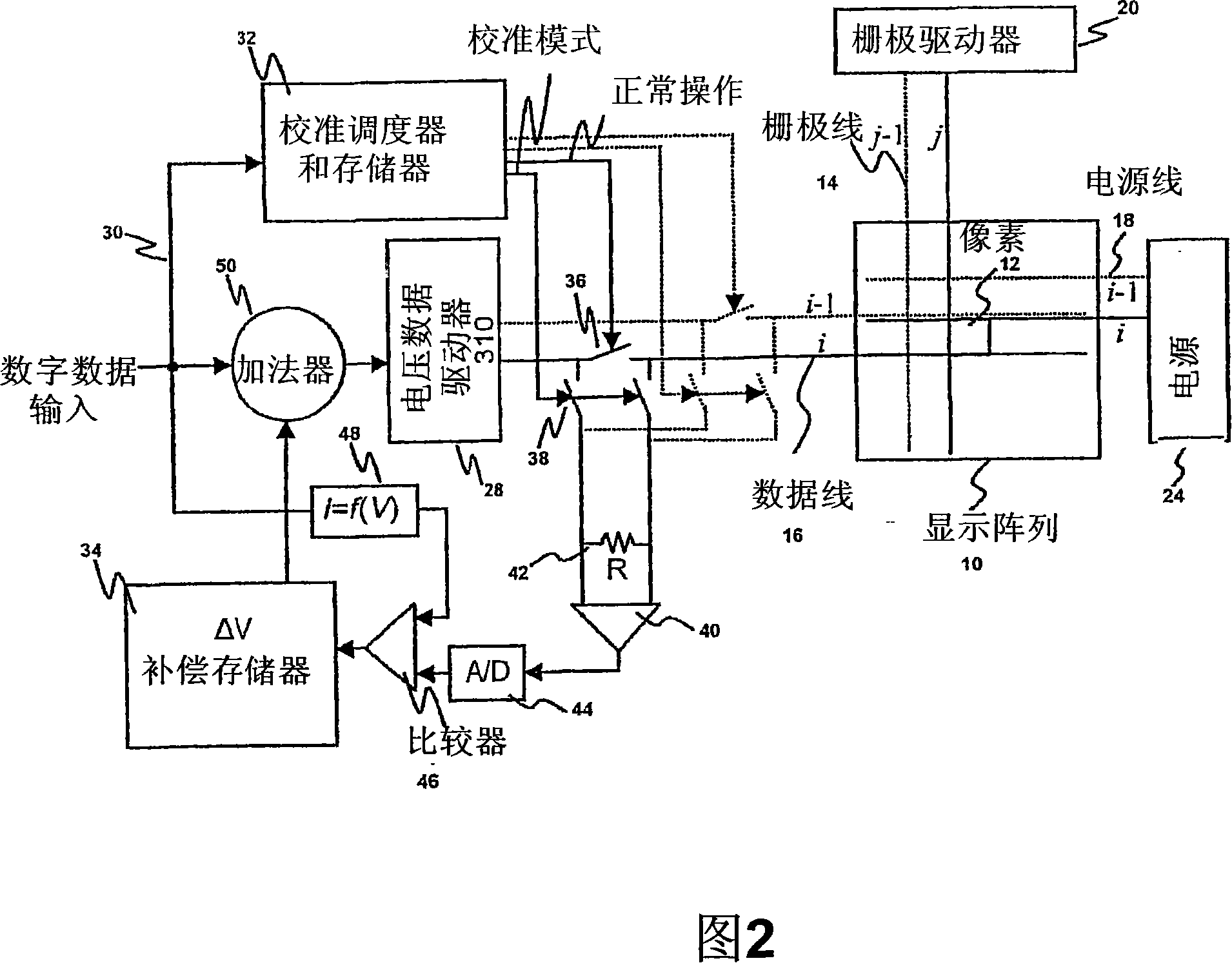
[0044] Embodiments of the present invention will now be described using a pixel including a light emitting device and a plurality of transistors. The light emitting device may be an organic light emitting diode (OLED). It should be noted that "pixel" and "pixel circuit" are used interchangeably.

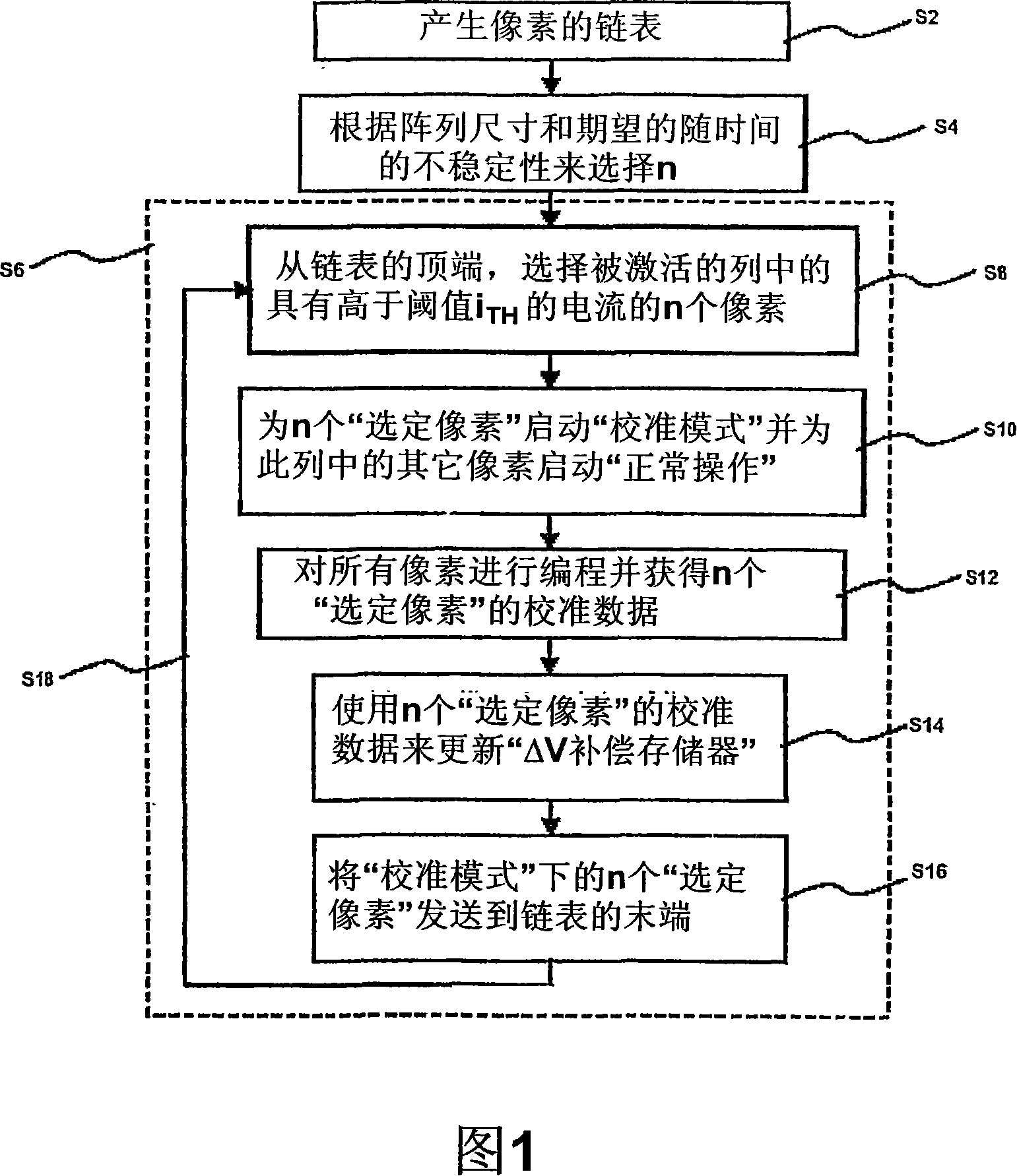
[0045] The real-time calibration schedule for a display array with multiple pixels is described in detail below. Figure 1 illustrates a calibration scheduling process according to one embodiment of the present invention. According to this technique, pixels are calibrated according to their aging and / or usage during normal operation of the display array.

[0046] A linked list of pixels is generated in step S2. The linked list contains the identification of pixels with high brightness for calibration. Use a linked list to schedule calibration priorities.

[0047] In step S4, "n" is selected according to the display size and the desired instability over time (eg shift of characteris...


PUM


Abstract

This invention presents a scheduling method and algorithm for calibration of pixels in active-matrix organic light-emitting diode (AMOLED) displays. The pixels are calibrated based on their aging and usage during the normal operation of active matrix display. The display data is used to determine the pixels with high brightness for calibration, which guarantees high speed and accurate calibration. This method can be used with any current programmed pixels, in particular, current mirror based designs.

Description

technical field [0001] The present invention relates to a display technology, and more particularly, to a method and system for programming, calibrating and driving a light emitting device display. Background technique [0002] Recently, active-matrix organic light-emitting diode (AMOLED) displays with amorphous silicon (a-Si), polysilicon, organic, or other driven backplanes have become more attractive due to their advantages over active-matrix liquid crystal displays. attraction. These include, for example, the use of a-Si, which has advantages of low production cost, high resolution, and wide viewing angle, in addition to its low-temperature fabrication enabling wide use of different substrates and flexible displays. [0003] An AMOLED display comprises an array of rows and columns of pixels in which organic light emitting diodes (OLEDs) and backplane electronics are arranged. Since OLED is a current-driven device, the pixel circuit of AMOLED should be able to provide a...

Claims


Application Information

Patent Timeline
Patent Type & Authority Applications(China)
IPC IPC(8): G09G3/20G09G3/32G09G3/3225
CPCG09G2320/0295G09G2320/043G09G3/3225G09G2320/0285
Inventor A·内森G·R·查吉P·塞尔瓦蒂
Owner IGNIS INNOVATION
Why Eureka
Try Eureka