
Voltage buffer and its source electrode driver

A technology of voltage buffer and current source, which is applied in the direction of instruments and static indicators, etc., can solve the problems of liquid crystal display display quality degradation, high load capacitance at the panel end, low slew rate of voltage buffer 100, etc., to improve the display picture Quality, improve the effect of turning rate

Active Publication Date: 2008-02-27
NOVATEK MICROELECTRONICS CORP
View PDF0 Cites 24 Cited by
  • Summary
  • Abstract
  • Description
  • Claims
  • Application Information

AI Technical Summary

Problems solved by technology

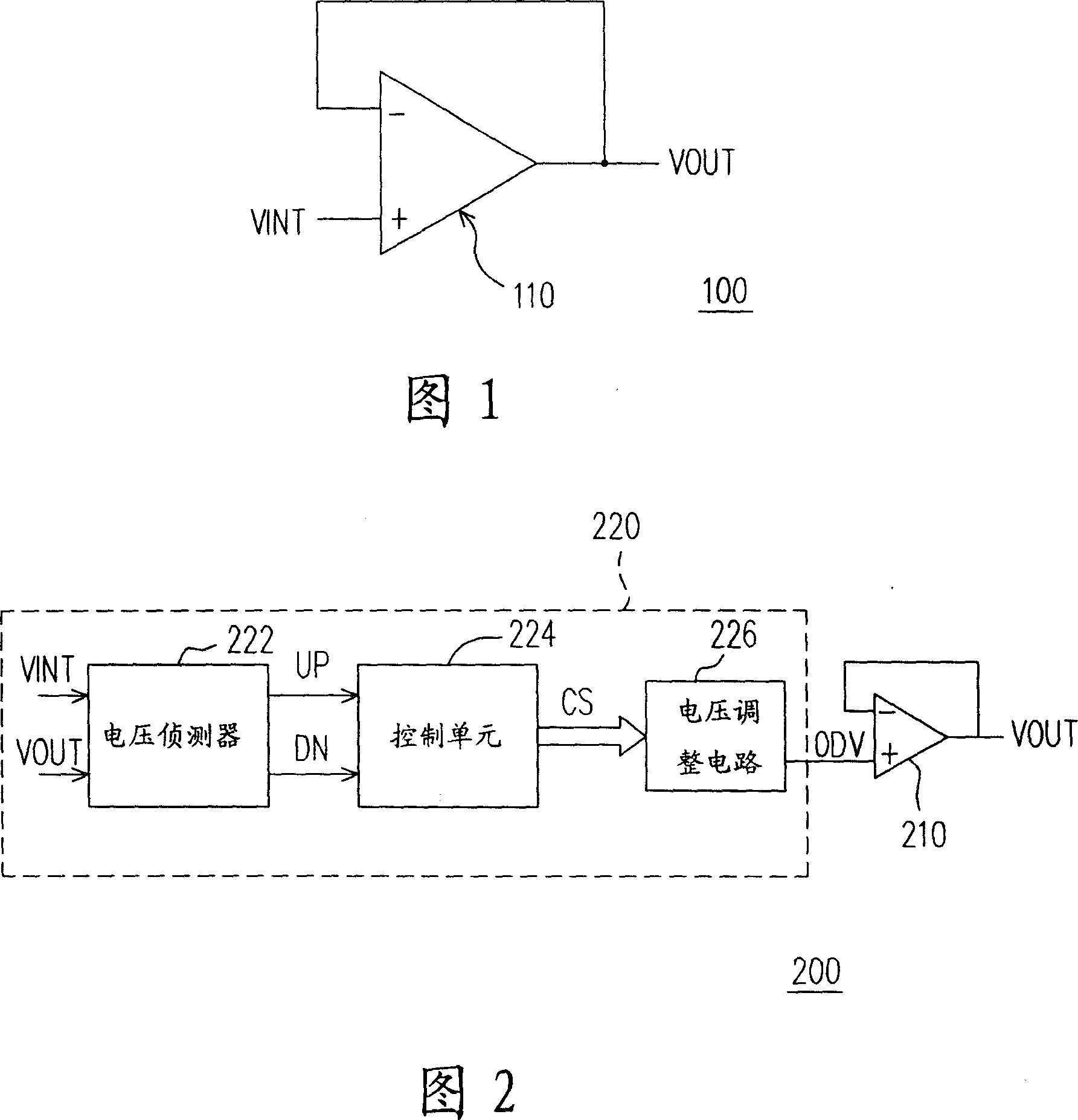
[0004] But when the voltage buffer shown in Figure 1 is applied to the source driver of the LCD, the load capacitance of the panel side required to be driven is relatively high
Therefore, when the input voltage VINT changes, the voltage buffer 100 cannot quickly adjust the output voltage VOUT to the same voltage level as the input voltage VINT due to the load.
That is, the slew rate (slew rate) of the voltage buffer 100 will become lower due to the load
[0005] As the size of the LCD becomes larger, the load capacitance becomes larger. If the slew rate of the voltage buffer used by the source driver cannot be effectively improved, the display quality of the LCD will decrease accordingly.

Method used


Image

  • Voltage buffer and its source electrode driver
  • Voltage buffer and its source electrode driver
  • Voltage buffer and its source electrode driver

Examples


Embodiment Construction

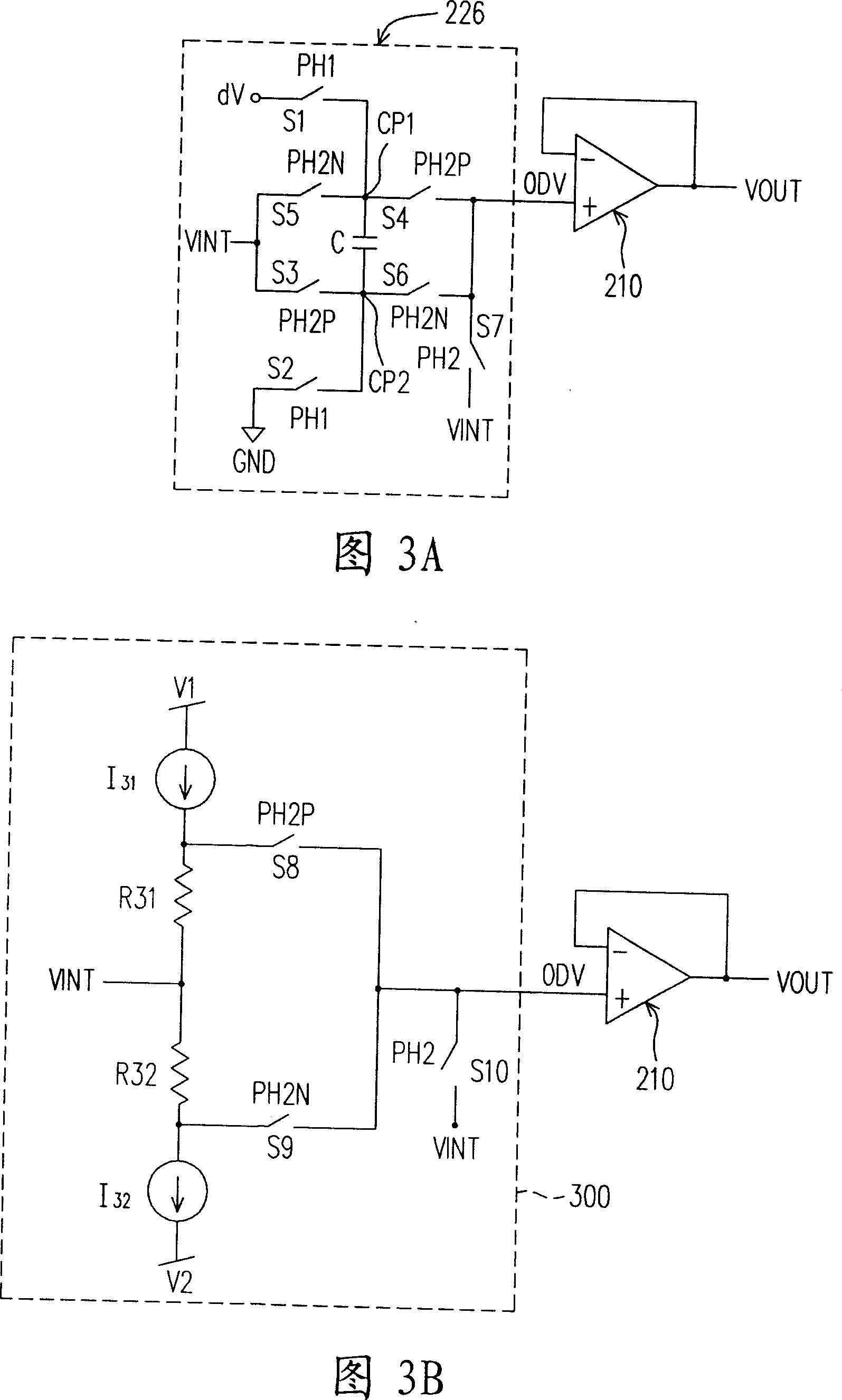
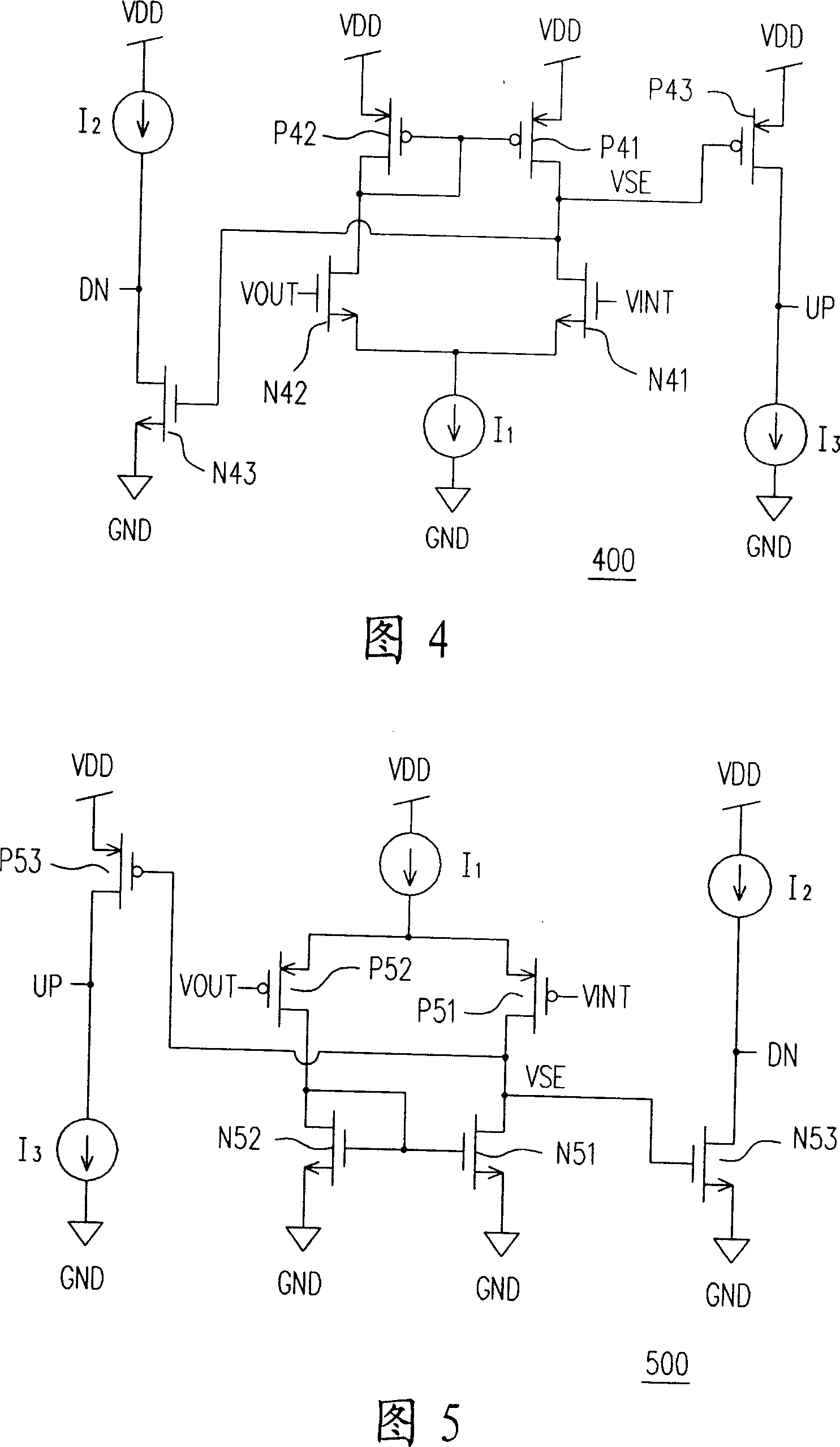
[0096] FIG. 2 is a circuit block diagram of a voltage buffer according to an embodiment of the invention. The voltage buffer 200 includes an operational amplifier 210 and an overdrive unit 220 . The operational amplifier 210 has a positive input terminal, a negative input terminal and an output terminal, and the output terminal is coupled to the negative input terminal to form a negative feedback structure. The voltage output by the output terminal is an output voltage VOUT. The overdrive unit 220 is coupled between an input voltage VINT and the operational amplifier 210 for comparing the input voltage VINT and the output voltage VOUT, and outputting an overdrive voltage ODV to the positive input terminal of the operational amplifier 210 .

[0097] Wherein, according to the comparison result of the overdrive unit 220, if the input voltage VINT is greater than the output voltage VOUT, then the overdrive voltage ODV is greater than the input voltage VINT; if the input voltage V...


PUM


Abstract

A pressure buffer and its source drivers, the said pressure buffer includes operation amplifier and overdrive cell, its operation amplifier output a output pressure. The overdrive cell couples between a output pressure and the operation amplifier, to compare the input pressure and the output one, and output a overdrive pressure to the positive output end of the operation amplifier. If the input pressure is bigger than the output pressure, the overdrive pressure is bigger than the input pressure, if the input pressure is smaller than the output pressure, the overdrive pressure is smaller than the input pressure, if the input pressure is equal to the output pressure, the overdrive pressure is equal to than the input pressure.

Description

technical field [0001] The present invention relates to a voltage buffer, and in particular to a voltage buffer with improved slew rate and its source driver. Background technique [0002] Traditional voltage buffers are usually used to transmit voltage signals and enhance their drive capability, while also preventing loads from affecting the output of the circuit. The voltage buffer used by the source driver in the liquid crystal display is usually formed by an operational amplifier. [0003] FIG. 1 is a circuit diagram of a voltage buffer according to a conventional art. FIG. 1 is a voltage buffer 100 with a negative feedback structure, and an output terminal of an operational amplifier 110 is coupled to its negative input terminal. The positive input terminal of the operational amplifier 110 is coupled to an input voltage VINT. Theoretically, due to the virtual short circuit, the output voltage VOUT generated by the output terminal of the operational amplifier 110 is e...

Claims


Application Information

Patent Timeline
IPC IPC(8): G09G3/36G09G3/20G02F1/133
Inventor 颜志仁
Owner NOVATEK MICROELECTRONICS CORP
Learn More