An output buffer for amoled column driver circuit

An output buffer, column drive technology, applied in the direction of logic circuit coupling/interface, logic circuit connection/interface arrangement, instrument, etc. using field effect transistors, to achieve the effect of large driving current and small quiescent current

Active Publication Date: 2018-07-20
SHANGHAI ADVANCED RES INST CHINESE ACADEMY OF SCI
View PDF4 Cites 2 Cited by
  • Summary
  • Abstract
  • Description
  • Claims
  • Application Information

AI Technical Summary

Problems solved by technology

[0005] In view of the above-mentioned shortcomings of the prior art, the object of the present invention is to provide an output buffer for an AMOLED column drive circuit, which is used to solve the problem that the output buffer in the prior art requires a comprehensive area when the load capacitance is further increased. , power consumption and other factors to further optimize the circuit

Method used


Image

  • An output buffer for amoled column driver circuit
  • An output buffer for amoled column driver circuit
  • An output buffer for amoled column driver circuit

Examples


Embodiment 1

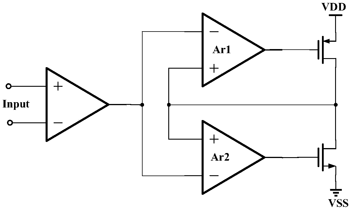
[0050] An output buffer for an AMOLED column drive circuit, comprising: a bias circuit 1, a rail-to-rail input stage circuit 2, a bootstrap stage circuit 3 and an output stage circuit 4, and the rail-to-rail input stage circuit 2 is respectively connected The bootstrap stage circuit 3 and the bias circuit 1 , the bootstrap stage circuit 3 is connected to the output stage circuit 4 . The rail-to-rail input stage circuit 2 is used to amplify the difference between the positive input signal and the reverse input signal; the bootstrap stage circuit 3 is used to increase the control voltage of the output stage circuit 4 to a level higher than The power supply voltage VDD may drop to be lower than the ground voltage VSS; the output stage circuit 4 is used to drive the output load; the bias circuit 1 is used to provide a bias voltage for the rail-to-rail input stage circuit 2 .

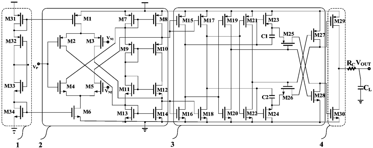
[0051] Such as image 3 As shown, in this embodiment, the rail-to-rail input stage circuit 2 includes a ...

Embodiment 2

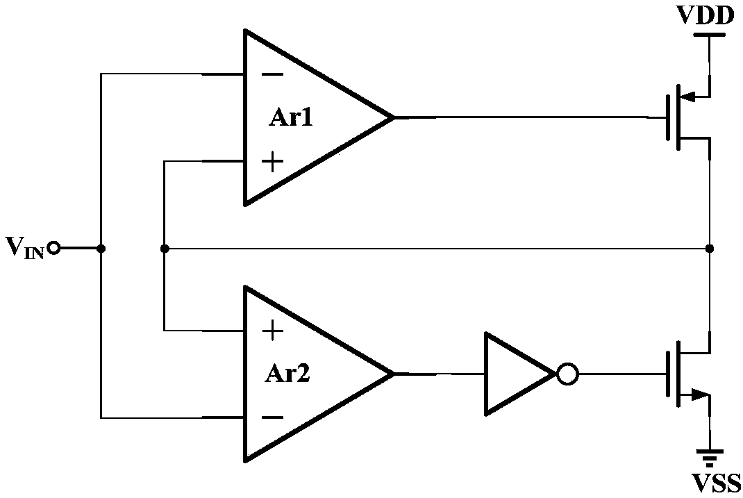
[0064] According to the first embodiment, the second embodiment is as image 3 As shown, the inverting input terminal V of the rail-to-rail input stage circuit 2 in this embodiment N Connected with the output buffer output signal Vout, the non-inverting input terminal V of the rail-to-rail input stage circuit 2 P with the input signal of the output buffer V IN connected together to form a unity gain buffer structure. Therefore, the signal can be simplified as the input signal V IN (V IN =V P ), the output signal V OUT (V OUT =V N ). According to the input signal V IN and the output signal V OUT , we divide the proposed circuit into the following working states.

[0065] (1) When the input signal V IN equal to the output signal V OUT (Static, V IN =V OUT ), the fifteenth transistor enters the saturation region, the sixteenth transistor enters the linear region, the seventeenth transistor enters the linear region, and the eighteenth transistor enters the saturatio...


PUM


Abstract

The invention provides an output buffer used for an AMOLED column driving circuit. The output buffer comprises a rail-to-rail input stage circuit, a bootstrapping stage circuit and an output stage circuit, wherein the rail-to-rail input stage circuit is connected with the bootstrapping stage circuit, the bootstrapping stage circuit is connected with the output stage circuit, and the rail-to-rail input stage circuit is used for amplifying non-inverting input signals and inverting input signals; the bootstrapping stage circuit is used for boosting a control voltage of the output stage circuit to be higher than a power supply voltage or bucking the control voltage to be lower than a ground voltage; and the output stage circuit is used for driving an output load. The output buffer provided by the invention is used for solving the problem that circuits needs to be further optimized by integrating factors such as area and power consumption when load capacitance of an output buffer in the prior art is further increased.

Description

technical field [0001] The invention relates to the technical field of plane display, in particular to an output buffer for an AMOLED column drive circuit. Background technique [0002] Compared with other display technologies, AMOLED display has the advantages of ultra-thin, wide viewing angle, low power consumption, fast response speed, natural color, etc., and is the most powerful competitor of the next-generation mainstream display technology. In the AMOLED display system, the column drive circuit is very important to realize high-speed, high-precision, low power consumption and high dynamic display drive. Usually, the column driving circuit includes a shift register, a sampling register, a data latch, a level conversion circuit, a digital-to-analog converter (Digital-to-Analog Converter, DAC) and an output buffer circuit. Among them, the output buffer determines the performance of the column driver circuit such as speed, precision, output range, and power consumption. ...

Claims


Application Information

Patent Timeline
Patent Type & Authority Patents(China)
IPC IPC(8): G09G3/3225H03K19/0185
CPCG09G3/3225G09G2310/0291H03K19/0185
Inventor 汪辉黄尊恺田犁章琦汪宁黄景林曹虎
Owner SHANGHAI ADVANCED RES INST CHINESE ACADEMY OF SCI
Why Eureka
Try Eureka