Thin silicon-on-insulator double-diffused metal oxide semiconductor transistor

a metal oxide semiconductor, double-diffused technology, applied in the direction of transistors, semiconductor devices, electrical equipment, etc., can solve the problems of compound semiconductor substrate cost very high, compound semiconductor high-voltage high-power devices, and compound semiconductor process is not compatible with silicon integrated circuit process, etc., to achieve low parasitic capacitance, reduce parasitic resistance, and high drive current

Inactive Publication Date: 2008-11-27
SHARP KK
View PDF3 Cites 20 Cited by
  • Summary
  • Abstract
  • Description
  • Claims
  • Application Information

AI Technical Summary

Benefits of technology

[0010]The present invention describes a new type of DMOS fabricated on SOI wafers. The active gate is fabricated on a very thin top silicon layer, which is compatible to Fully Depleted SOI technology (FD SOI), and the drain drift area has thicker top silicon film so that the drain parasitic resistance is reduced. The fully depleted active channel area results a very small parasitic capacitance. This device provides a high drive current comparable to conventional DMOS designs, but with a much lower on resistance and much smaller device area. The starting wafer is a standard commercially available SOI wafers. The device structure and the processes are also compatible with FD SOI technology. The device is individually island isolated and has very small depletion region volume. Therefore, high frequency, small area, high voltage, and low leakage current devices can be achieved. Although FD SOI compatibility is described in this application, depending on the device tuning, the present invention is also compatible with the fabrication of partially depleted (PD) SOI devices. The advantages associated with using FDSOI devices are also applicable to PDSOI devices. More particularly, the present invention active gate is compatible with FDSOI and PDSOI devices, depending on device tuning.

Problems solved by technology

One limitation of a conventional planar MOS device is that the channel length, is proportional to the breakdown voltage, but inversely proportional to current.
Compound semiconductor substrate costs are very high.
In addition, the compound semiconductor processes are not compatible with silicon integrated circuit processes.
As a result, the cost of compound semiconductor high voltage high power devices is very high and, therefore, not suitable for consumer applications.
The depletion area of the DMOST, whether it is back output or front output device, is also very large.
Thus, the bulk silicon DMOST is not suitable for high temperature high voltage applications.
Since conventional DMOS and bipolar transistor designs both require thick silicon films, these designs fail to make use of all the above-mentioned potential advantages available with the use of SOI substrate.
Since the leakage current is proportional to the volume of the junction depletion region, these thick top active silicon films generate high leakage currents, which are especially problematic at high temperatures.
Further, since conventional commercially available SOI wafers are fabricated with less than a 1.5 μm top active silicon film thickness, the above-mentioned thick-film designs require a high cost, custom type of SOI wafer.

Method used


Image

  • Thin silicon-on-insulator double-diffused metal oxide semiconductor transistor
  • Thin silicon-on-insulator double-diffused metal oxide semiconductor transistor
  • Thin silicon-on-insulator double-diffused metal oxide semiconductor transistor

Examples


Embodiment Construction

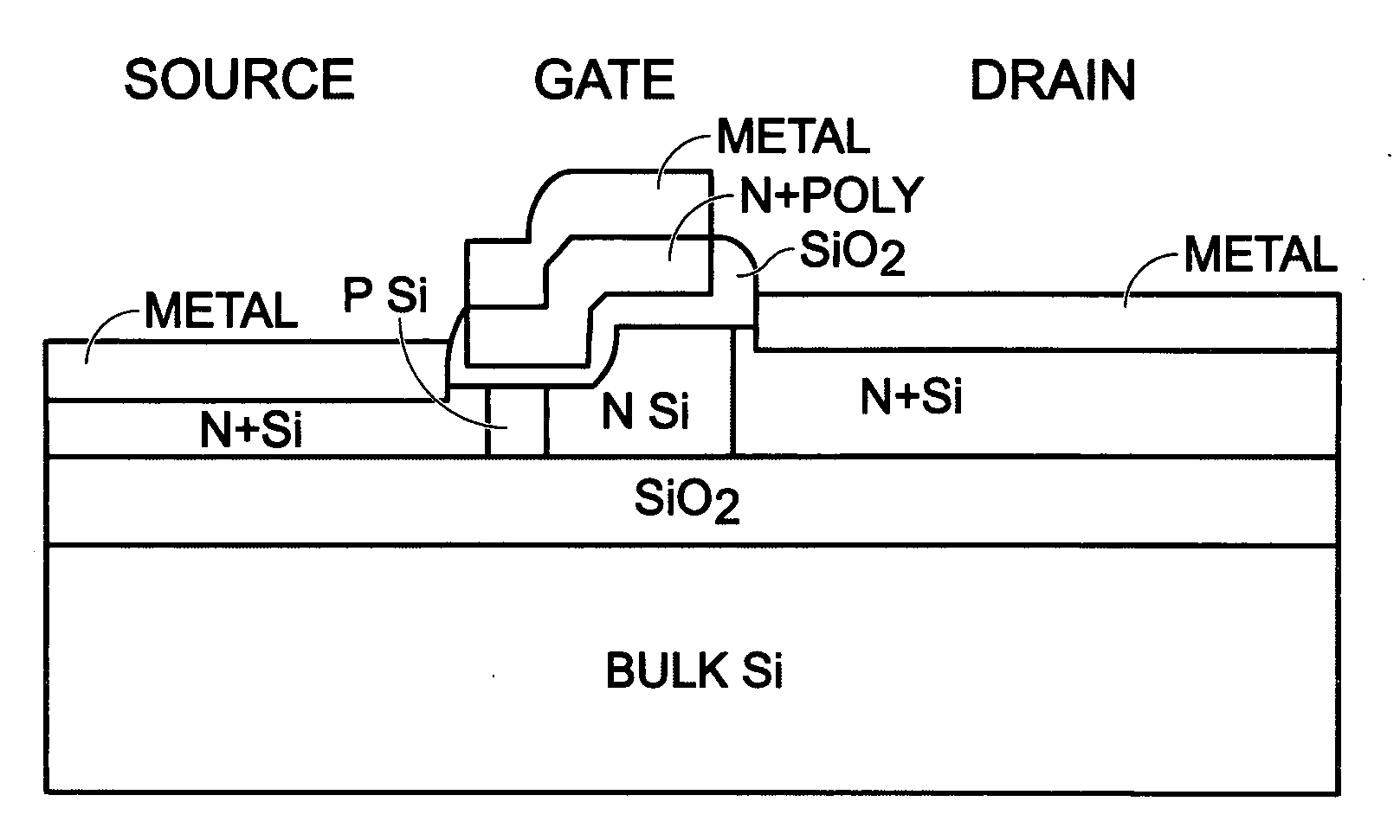
[0018]FIG. 2 is a partial cross-sectional view of a silicon (Si)-on-insulator (SOI) double-diffused metal oxide semiconductor transistor (DMOST) with a stepped channel thickness. The DMOST 200 comprises a SOI substrate 202 with a Si top layer 204. A source region 206 is formed in an area 208 of the Si top layer having a first thickness 210. A drain region 212 is formed in an area 214 of the Si top layer having a second thickness 216, greater than the first thickness. A channel 218 has the first thickness area 220 adjacent the source region 206 with a first-type dopant, a second thickness area 222 adjacent the drain region 212, and a sloped thickness 224 between the first and second thicknesses. The second and sloped thickness areas of the channel have a second-type dopant, opposite of the first-type dopant. For example, if the first dopant is p-type, the second dopant is n-type. A stepped gate 226 overlies the channel 218.

[0019]In one aspect, the source region first thickness 210 is...


PUM


Abstract

A method is provided for fabricating a silicon (Si)-on-insulator (SOI) double-diffused metal oxide semiconductor transistor (DMOST) with a stepped channel thickness. The method provides a SOI substrate with a Si top layer having a surface. A thinned area of the Si top layer is formed, and a source region is formed in the thinned Si top layer area. The drain region is formed in an un-thinned area of the Si top layer. The channel has a first thickness adjacent the source region with first-type dopant, and a second thickness, greater than the first thickness, adjacent the drain region. The channel also has a sloped thickness between the first and second thicknesses. The second and sloped thicknesses have a second-type dopant, opposite of the first-type dopant. A stepped gate overlies the channel.

Description

BACKGROUND OF THE INVENTION[0001]1. Field of the Invention[0002]This invention generally relates to integrated circuit (IC) fabrication and, more particularly, to a double-diffused metal oxide semiconductor transistor (DMOST) with a multi-thickness channel fabricated on SOI for medium power device applications.[0003]2. Description of the Related Art[0004]FIG. 1 is a partially cross-sectional view of a vertical output DMOST device with substrate contact to the drain output (prior art). One limitation of a conventional planar MOS device is that the channel length, is proportional to the breakdown voltage, but inversely proportional to current. That is, high current planar devices require a very short channel length and, therefore, have a very low breakdown voltage. To address this short channel limitation, DMOST devices were developed. A DMOST device is formed by a double-diffusion. For example, an n-channel DMOST is conventionally formed by a deep p+ implant, followed by a shallow n+...

Claims


Application Information

Patent Timeline
Patent Type & Authority Applications(United States)
IPC IPC(8): H01L29/786H01L21/336
CPCH01L29/0657H01L29/42368H01L29/66689H01L29/7824H01L29/78624H01L29/78696
Inventor HSU, SHENG TENGLEE, JONG-JAN
Owner SHARP KK
Why Eureka
Try Eureka