Optical semiconductor device

a semiconductor and optical technology, applied in semiconductor lasers, laser optical resonator construction, laser details, etc., can solve the problems of increasing the width of the effective active layer, a disadvantageous structure for increasing the relaxation oscillation frequency, etc., and achieves high relaxation oscillation frequency, low threshold current, and high reliability

Active Publication Date: 2013-08-15
LUMENTUM JAPAN INC
View PDF18 Cites 11 Cited by
  • Summary
  • Abstract
  • Description
  • Claims
  • Application Information

AI Technical Summary

Benefits of technology

[0015]An object of the present invention is to provide a semiconductor laser which uses InGaAlAs in an active layer and has long-term reliability since a threshold current is small, a relaxation oscillation frequency at a low driving current is high, and temperature characteristics are good. Another object of the present invention is to provide a semiconductor laser showing a stable operation in a state where a transverse mode is a base mode in addition to the above description. In addition, still another object of the present invention is to provide a semiconductor laser which has small parasitic capacitance and can be operated at high speed in addition to the above description. Further, still another object of the present invention is to provide an optical semiconductor device having the above-described structures.
[0024]Therefore, according to the optical semiconductor device of the present invention, it is possible to realize a low threshold current, a high relaxation oscillation frequency, and high reliability in a BH laser which has an active layer including Al-based elements.

Problems solved by technology

The ridge type laser can be said to be a disadvantageous structure for increasing the relaxation oscillation frequency fr since the effective driving current is reduced by the influence of the reactive current due to the diffusion current in the transverse direction and thus the width of the effective active layer also increases.

Method used


Image

  • Optical semiconductor device
  • Optical semiconductor device
  • Optical semiconductor device

Examples


embodiment 1

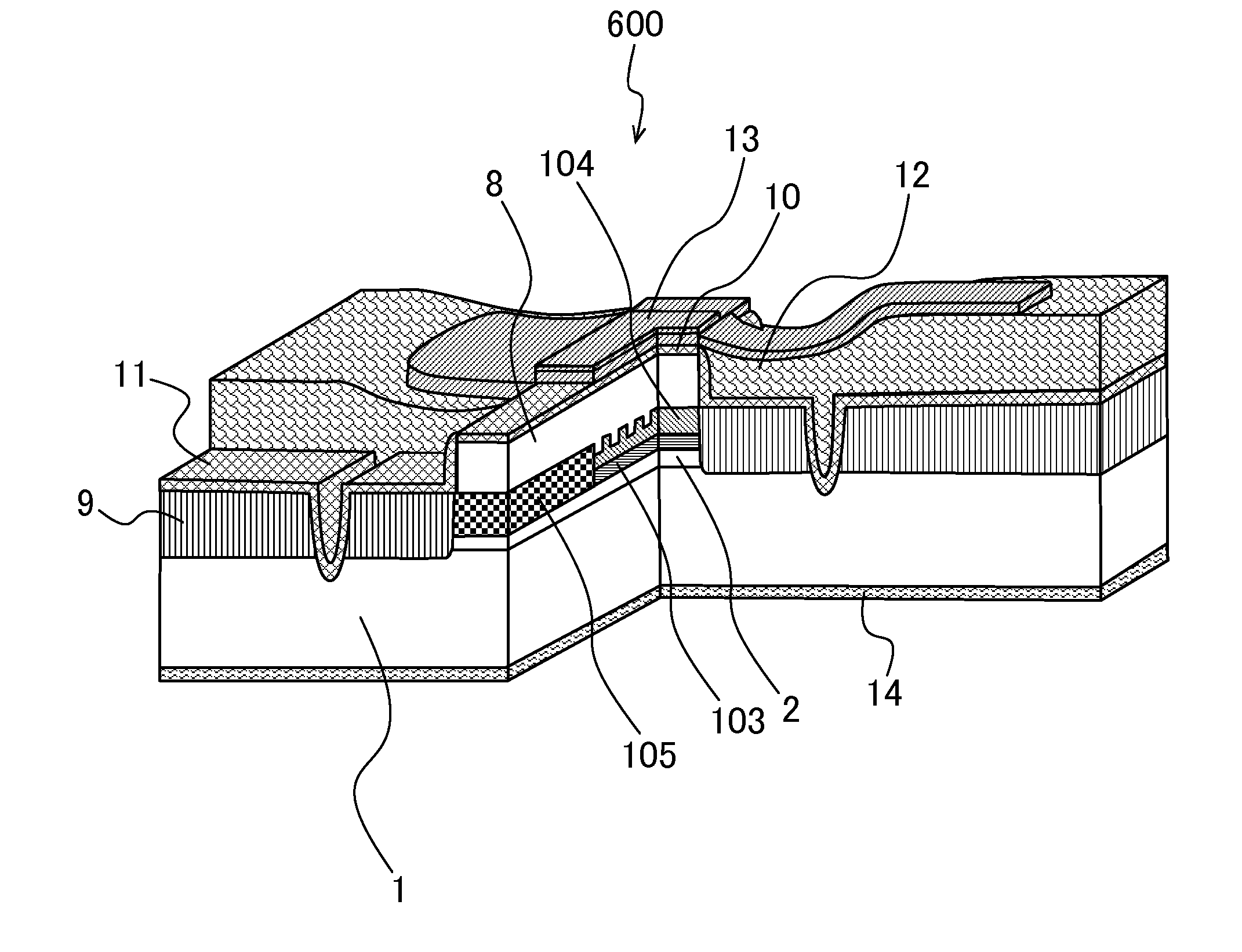
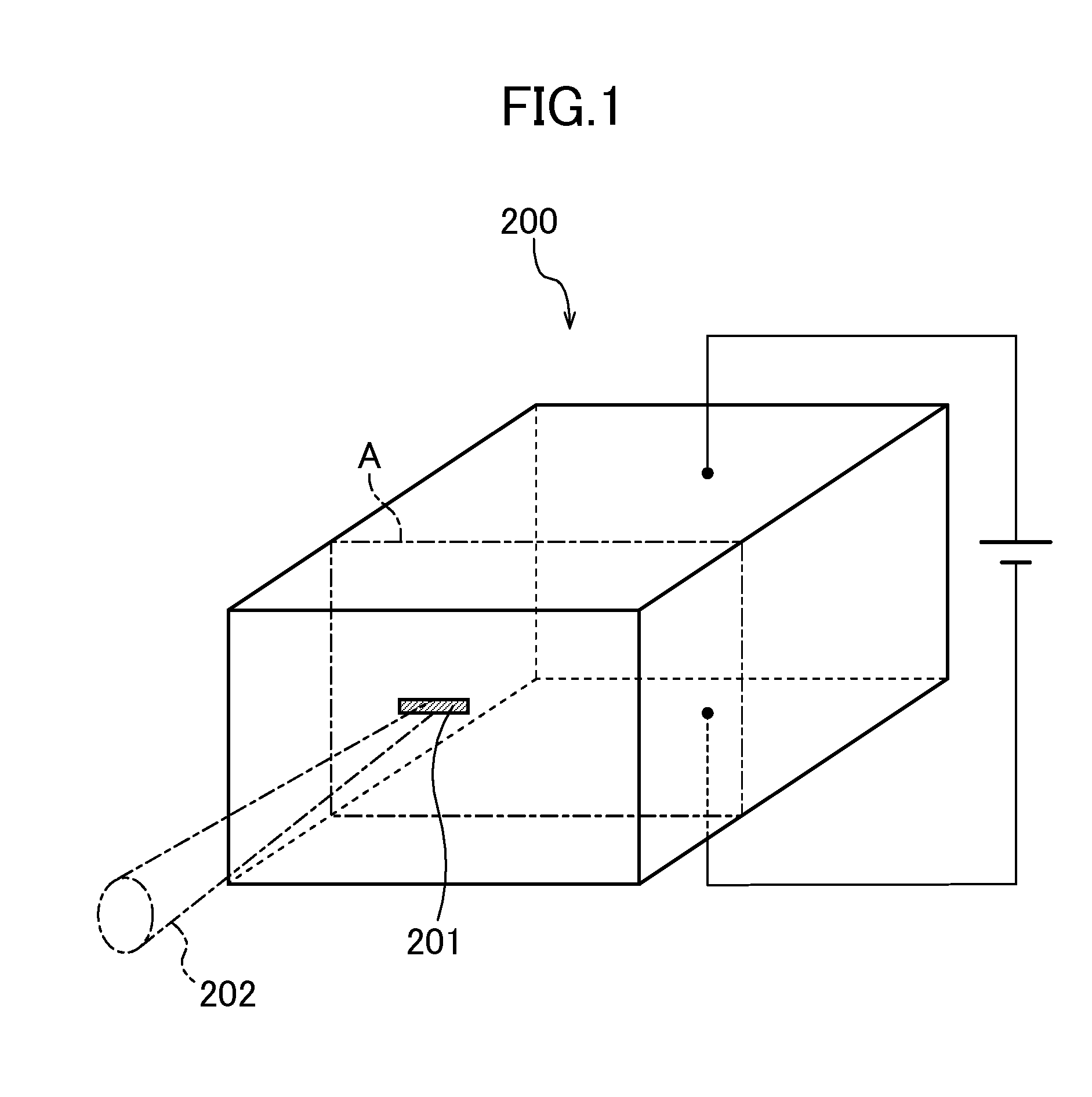
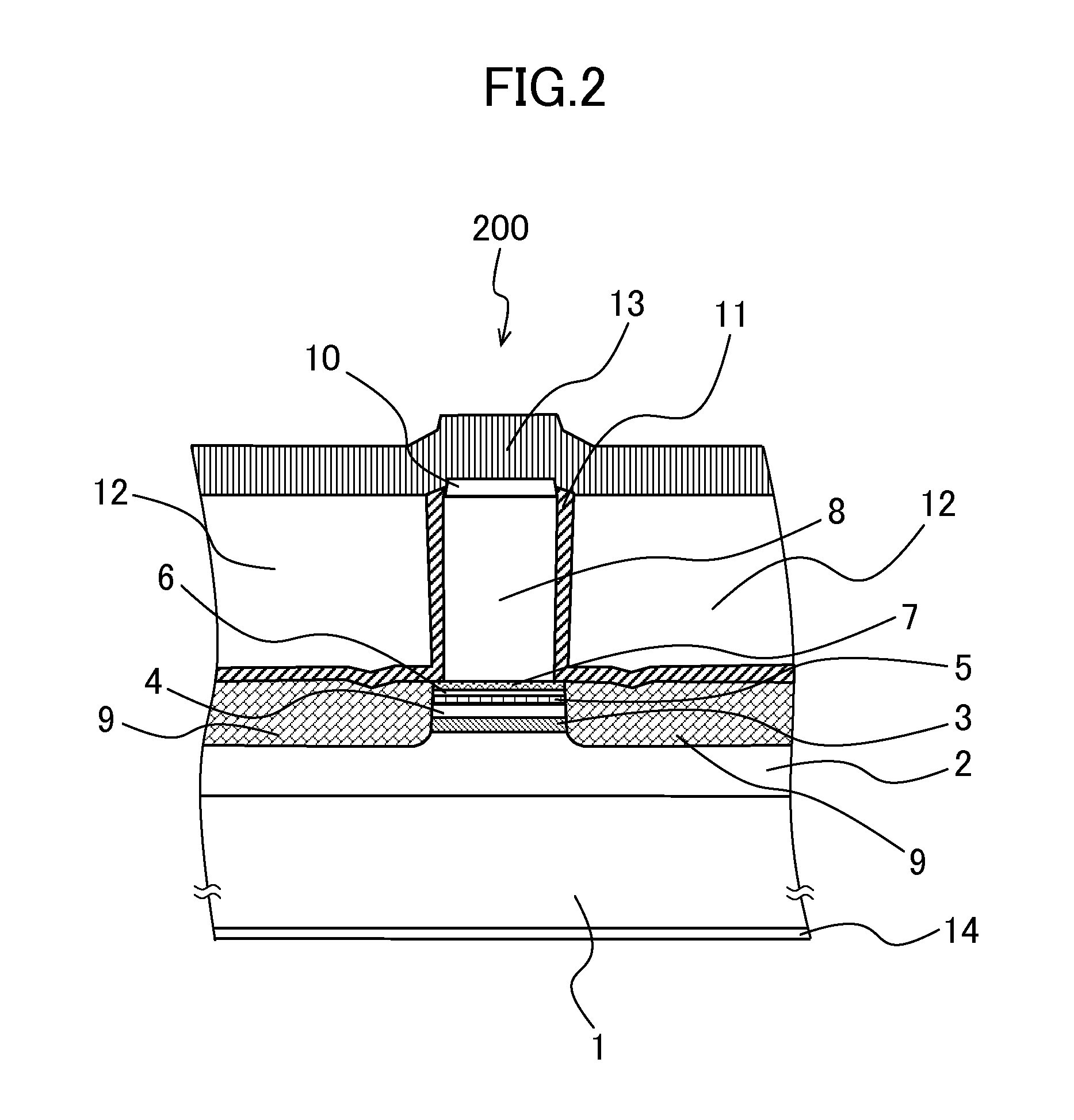
[0049]FIG. 1 schematically shows a semiconductor laser device 200 which is an optical semiconductor device related to Embodiment 1 of the present invention. As shown in this figure, the semiconductor laser device 200 is a device where laser light 202 is oscillated from an oscillation region 201 by applying voltages to two electrodes provided in opposite surfaces of a rectangular parallelepiped.

[0050]FIG. 2 is a cross-sectional view in the cross-section indicated by A of FIG. 1, and is a schematic diagram of the cross-section perpendicular to an optical axis of a semiconductor laser which is oscillated in a 1.3 μm band of an optical fiber communication transmission light source. As shown in this figure, the semiconductor laser device 200 includes an n type InP substrate 1; an n type InP buffer layer 2 which is a lower clad layer of which the doping concentration is 1×1018 cm−3 and the thickness is 500 nm; an n type InGaAlAs-SCH layer 3, disposed under MQW, of which the doping concent...

embodiment 2

[0070]FIG. 9 is a diagram illustrating a semiconductor laser device 300 which is an optical semiconductor device according to Embodiment 2 of the present invention, and is a schematic diagram of the cross-section perpendicular to an optical axis of a DFB semiconductor laser which is oscillated in a 1.3 μm band of an optical fiber communication transmission light source. As shown in this figure, the semiconductor laser device 300 includes a p type InP substrate 71; a p type InP buffer layer 72 which is a lower clad layer of which the doping concentration is 1×1018 cm−3 and the thickness is 2 μm; a p type InAlAs electron stop layer 73 of which the doping concentration is 1×1018 cm−3 and the thickness is 50 nm; a p type InGaAlAs-SCH layer 74, disposed under MQW, of which the doping concentration is 1×1018 cm−3, the thickness is 50 nm, and the composition wavelength is 0.94 μm; a strained InGaAlAs-MQW layer 75 which has a well layer 9 nm thick and a barrier layer 10 nm thick in five cyc...

embodiment 3

[0077]FIG. 14 is a diagram illustrating a semiconductor laser device 400 which is an optical semiconductor device according to Embodiment 3 of the present invention, and is a schematic diagram of the cross-section perpendicular to an optical axis of a DFB semiconductor laser which is oscillated in a 1.3 μm band of an optical fiber communication transmission light source. The present embodiment is similar to Embodiment 2, and relates to a DFB laser formed on the p type InP substrate 71. A difference is that an n type SCH layer 99 is made of InGaAsP. The n type SCH layer 99 is made of not InGaAlAs but InGaAsP, thus a band structure of the interface with the burial layer is not of Type-II shown in FIG. 7 or 8 but Type-I, and thereby electrons on the conduction band side in the SCH layer are efficiently confined without leaking to the burial layer. The burial layer may have the shift burial structure described in Embodiment 2, and favorably constricts electrons therein according to the ...


PUM


Abstract

In a BH laser which uses InGaAlAs-MQW in an active layer, Al-based semiconductor multi-layer films including an InP buffer layer and an InGaAlAs-MQW layer, and an InGaAsP etching stop layer are formed in a mesa shape, and a p type InP burial layer is buried in side walls of the mesa shape. An air ridge mesa-stripe of a lateral center that is substantially the same as that of the mesa shape is formed on the mesa shape. According to the present structure, a leakage current can be considerably reduced, the light confinement coefficient can be made to be larger than in a BH laser in the related art, and thereby it is possible to implement a semiconductor laser with a low leakage current and a high relaxation oscillation frequency.

Description

CROSS-REFERENCE TO RELATED APPLICATION[0001]The present application claims priority from Japanese application JP2012-026749 filed on Feb. 9, 2012, the content of which is hereby incorporated by reference into this application.BACKGROUND OF THE INVENTION[0002]1. Field of the Invention[0003]The present invention relates to an optical semiconductor device which is a laser device using a semiconductor, and particularly to a communication semiconductor laser used as a transmission light source of an optical fiber.[0004]2. Description of the Related Art[0005]The Internet becomes established as an infrastructure which is vital for modern society from the business to the home life, and enlarges its range of applications from data communication and blogs to mail order sales, moving pictures, electronic books, SNS (Social Network Service), and the like. With the enlargement of the range of applications, the traffic volume of the optical network supporting the Internet keeps on increasing. The...

Claims


Application Information

Patent Timeline
Patent Type & Authority Applications(United States)
IPC IPC(8): H01S5/34H01S5/12
CPCH01S5/3403B82Y20/00H01S5/0287H01S5/12H01S5/2201H01S5/2206H01S5/2222H01S5/2226H01S5/2275H01S5/3095H01S5/3201H01S5/3213H01S5/34306H01S5/209H01S5/2213H01S5/2224H01S2301/176H01S5/0021
Inventor NAKAHARA, KOUJIWAKAYAMA, YUKIKITATANI, TAKESHISHINODA, KAZUNORI
Owner LUMENTUM JAPAN INC
Why Eureka
Try Eureka