This helps you quickly interpret patents by identifying the three key elements:
Problems solved by technology
Method used
Benefits of technology
Benefits of technology
The present invention provides an ESD protection device that reduces the impact of diode capacitance, which helps to maintain the device's circuit characteristics. Additionally, the invention minimizes stray capacitance between post-shaped electrodes, resulting in a smaller, more efficient ESD protection device with excellent high-frequency performance.
Problems solved by technology
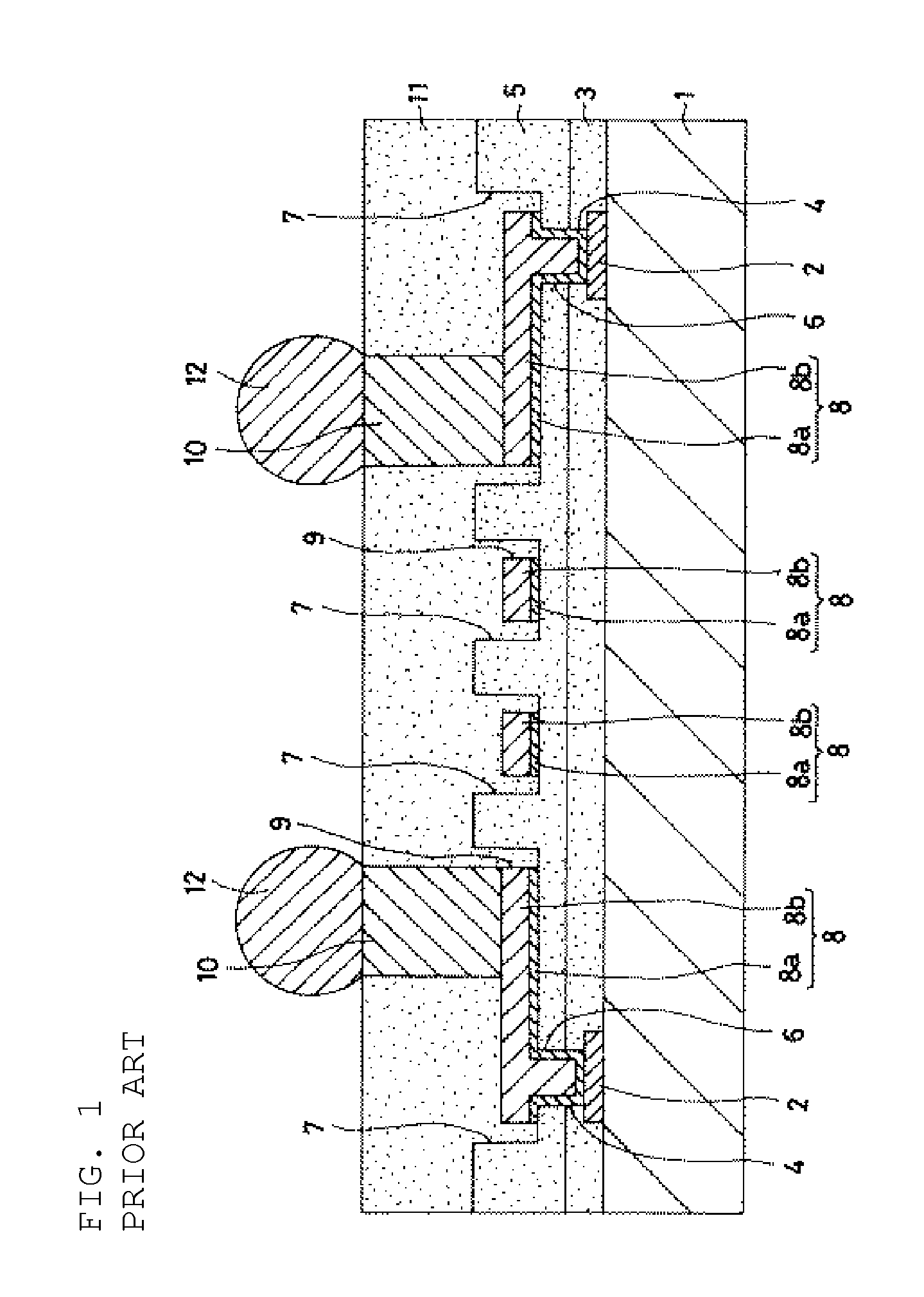
Such semiconductor integrated circuits, which are constant-voltage driven circuits formed of fine wiring patterns formed on semiconductor substrates, are in general vulnerable to electrostatic discharges such as surges.
There is a problem in that when such an ESD protection device is provided in a high-frequency circuit, an influence from the parasitic capacitance of the diode exists.
In other words, as a result of an ESD protection device being inserted in a signal line, the impedance is changed due to an influence from the parasitic capacitance of the diode, and this may cause signal loss.
However, an existing ESD protection device such as the one illustrated in FIG. 1 may structurally cause parasitic capacitance to be generated between the electrodes, in addition to the parasitic capacitance of the diode, and this may result in an increase in the capacitance of the ESD protection device itself.
Method used
Image
Click on the blue label to locate the original text in one second.
Reading with bidirectional positioning of images and text.
Examples
first preferred embodiment
[0037]An ESD protection device according to preferred embodiments of the present invention is described with reference to the figures.
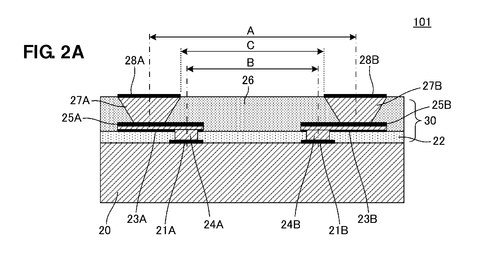
[0038]FIG. 2A is a cross-sectional view of the major portions of an ESD protection device 101 according to the first preferred embodiment. FIG. 2B is a top view of the ESD protection device 101. FIG. 3 is a perspective view of the ESD protection device 101.
[0039]Referring to FIG. 2A, the ESD protection device 101 includes a semiconductor substrate 20 including input / output electrodes 21A and 21B, and a rewiring layer 30 provided on the top surface of the semiconductor substrate 20. Although not illustrated in FIG. 2A, an ESD protection circuit is provided in the top layer of the semiconductor substrate 20, and the input / output electrodes 21A and 21B are connected to the ESD protection circuit. The rewiring layer 30 includes interlayer wiring lines 24A and 24B, in-plane wiring lines 25A and 25B, and post-shaped electrodes 27A and 27B.
[0040]First ends o...
second preferred embodiment
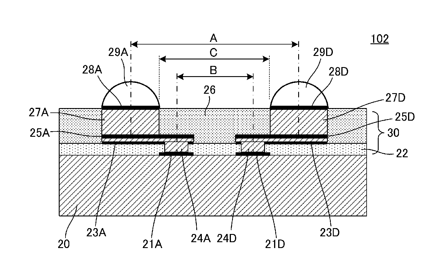
[0062]FIG. 8A is a cross-sectional view of the major portions of an ESD protection device 102 according to a second preferred embodiment of the present invention. FIG. 8B is a plan view seen from the mounting surface side of the device. FIG. 8A is a cross-sectional view taken along line X-X illustrated in FIG. 8B.
[0063]The ESD protection device 102 includes a semiconductor substrate 20 including input / output electrodes 21A and 21D and a rewiring layer 30 located on the top surface of the semiconductor substrate 20. Although not illustrated in FIG. 8A and FIG. 8B, an ESD protection circuit is provided in the top layer of the semiconductor substrate 20 and input / output electrodes (21A, 21D, and the like) are connected to the ESD protection circuit. The rewiring layer 30 includes interlayer wiring lines (24A, 24D, and the like), in-plane wiring lines (25A, 25D, and the like), and post-shaped electrodes (27A, 27D, and the like).
[0064]The cross-sectional structure illustrated in FIG. 8A ...
third preferred embodiment
[0070]FIG. 11 is a cross-sectional view of the major portions of an ESD protection device 103 according to a third preferred embodiment of the present invention. In the ESD protection device 103, post-shaped electrodes 27A and 27B are exposed on the sides of the device, and terminal electrodes 28A and 28B defined by metal plating are located on the surfaces of the sides. In other words, the terminal electrodes 28A and 28B which continuously extend from the bottom surface (upper surface in the orientation illustrated in FIG. 11) to the side surfaces of the ESD protection device are provided.
[0071]By providing terminal electrodes having such configurations, when the ESD protection device 103 is mounted on a motherboard, solder extends to the side surfaces of the terminal electrodes 28A and 28B such that the contact areas between the solder and the terminal electrodes 28A and 28B are increased. As a result, the connection strength of the ESD protection device 103 is increased and it be...
PUM
Abstract
An ESD protection device includes a semiconductor substrate including input / output electrodes and a rewiring layer located on the top surface of the semiconductor substrate. An ESD protection circuit is provided in the top layer of the semiconductor substrate, and the input / output electrodes are connected to the ESD protection circuit. The rewiring layer includes interlayer wiring lines, in-plane wiring lines, and post-shaped electrodes. First ends of the interlayer wiring lines provided in the thickness direction are connected to the input / output electrodes provided on the top surface of the semiconductor substrate and the second ends are connected to first ends of the in-plane wiring lines extending in the plane direction. The distance between the centers of the first and second post-shaped electrodes is larger than the distance between the centers of the first and second input / output electrodes.
Description
BACKGROUND OF THE INVENTION[0001]1. Field of the Invention[0002]The present invention relates to ESD protection devices that protect, for example, semiconductor ICs from static electricity, and in particular to CSP-type ESD protection devices whose functional portions are provided on silicon substrates.[0003]2. Description of the Related Art[0004]Various electronic apparatuses, such as mobile communication terminals, digital cameras, and notebook PCs include semiconductor integrated circuits (IC chips) that form logic circuits, memory circuits, and the like. Such semiconductor integrated circuits, which are constant-voltage driven circuits formed of fine wiring patterns formed on semiconductor substrates, are in general vulnerable to electrostatic discharges such as surges. Hence, electrostatic discharge (ESD) protection devices are used to protect these semiconductor integrated circuits from electrostatic discharges.[0005]As disclosed in Japanese Unexamined Patent Application Publi...
Claims
Application Information
Patent Timeline
Application Date:The date an application was filed.
Publication Date:The date a patent or application was officially published.
First Publication Date:The earliest publication date of a patent with the same application number.
Issue Date:Publication date of the patent grant document.
PCT Entry Date:The Entry date of PCT National Phase.
Estimated Expiry Date:The statutory expiry date of a patent right according to the Patent Law, and it is the longest term of protection that the patent right can achieve without the termination of the patent right due to other reasons(Term extension factor has been taken into account ).
Invalid Date:Actual expiry date is based on effective date or publication date of legal transaction data of invalid patent.

