Semiconductor device with dual damascene wiring

a technology of damascene and semiconductor devices, which is applied in the direction of semiconductor devices, semiconductor/solid-state device details, electrical apparatus, etc., can solve the problems of low signal transmission speed, and difficult etching of cu, so as to achieve less damage to the underlying conductive region

Inactive Publication Date: 2006-10-10
TRINITY SEMICON RES
View PDF27 Cites 13 Cited by
  • Summary
  • Abstract
  • Description
  • Claims
  • Application Information

AI Technical Summary

Benefits of technology

[0100]FIG. 1F shows the second etch stopper layer 14 exposed because the second interlayer insulating film 15 on the bottom of the wiring trench is etched by the process of etching the first etch stopper layer 12 shown in FIG. 1D. As the second etch stopper layer 14 is exposed, parasitic capacitance of the wiring layer increases slightly. However, the surface of the conductive region 11 is prevented from being damaged and abnormal etching is prevented, these advantageous effects being retained.
[0101]A supplemental description will be given relative to a preferred height of the second etch stopper layer 14. It is assumed that the thickness of the interlayer insulating film excluding the second etch stopper layer 14 is, for example, 1500 nm. A wiring trench having a depth of 800 nm is formed in this interlayer insulating film. The height of the protective filler is assumed to be 600 nm.
[0102]FIG. 17AA is a schematic cross sectional view of a substrate having a wiring trench of 800 nm in depth formed without using the second etch stopper layer 14. The shoulder near the via hole is fairly etched and abnormal etching occurs in the area around the filler 55.
[0103]FIG. 17BA shows the state that the resist pattern PR2 and filler 55 were removed. The interlayer insulating film has a sharp projection and a deep cut near the via hole. It is difficult to form a dual damascene wiring layer.
[0104]FIG. 17AB shows the state that the etch stopper layer is disposed at a height of 200 nm from the bottom of the interlayer insulating film. Also in this case, the shoulder near the via hole is fairly etched, the upper surface of the filler 55 projects higher than the etched surface of the interlayer insulating film, and abnormal etching occurs in the nearby area.
[0105]FIG. 17BB shows the state that the resist pattern PR2 and filler 55 were removed. The interlayer insulating film has a sharp projection and a deep cut near the via hole.

Problems solved by technology

An increase in the capacitance or resistance lowers a signal transmission speed in the conductive wire and hinders speeding up the device operation.
Cu is difficult to be patterned by etching.
With the via first dual damascene process, there is a possibility that the etch stopper layer on the bottom of the via hole is damaged so that the underlying conductive region is damaged.
As described above, unless a filler is used, a conventional dual damascene process is not always easy to sufficiently protect the surface of a conductive region disposed under a dual damascene wiring pattern and form a highly reliable wiring structure.

Method used


Image

  • Semiconductor device with dual damascene wiring
  • Semiconductor device with dual damascene wiring
  • Semiconductor device with dual damascene wiring

Examples


first embodiment

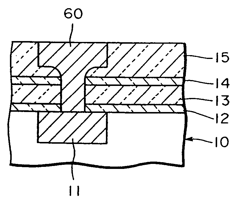
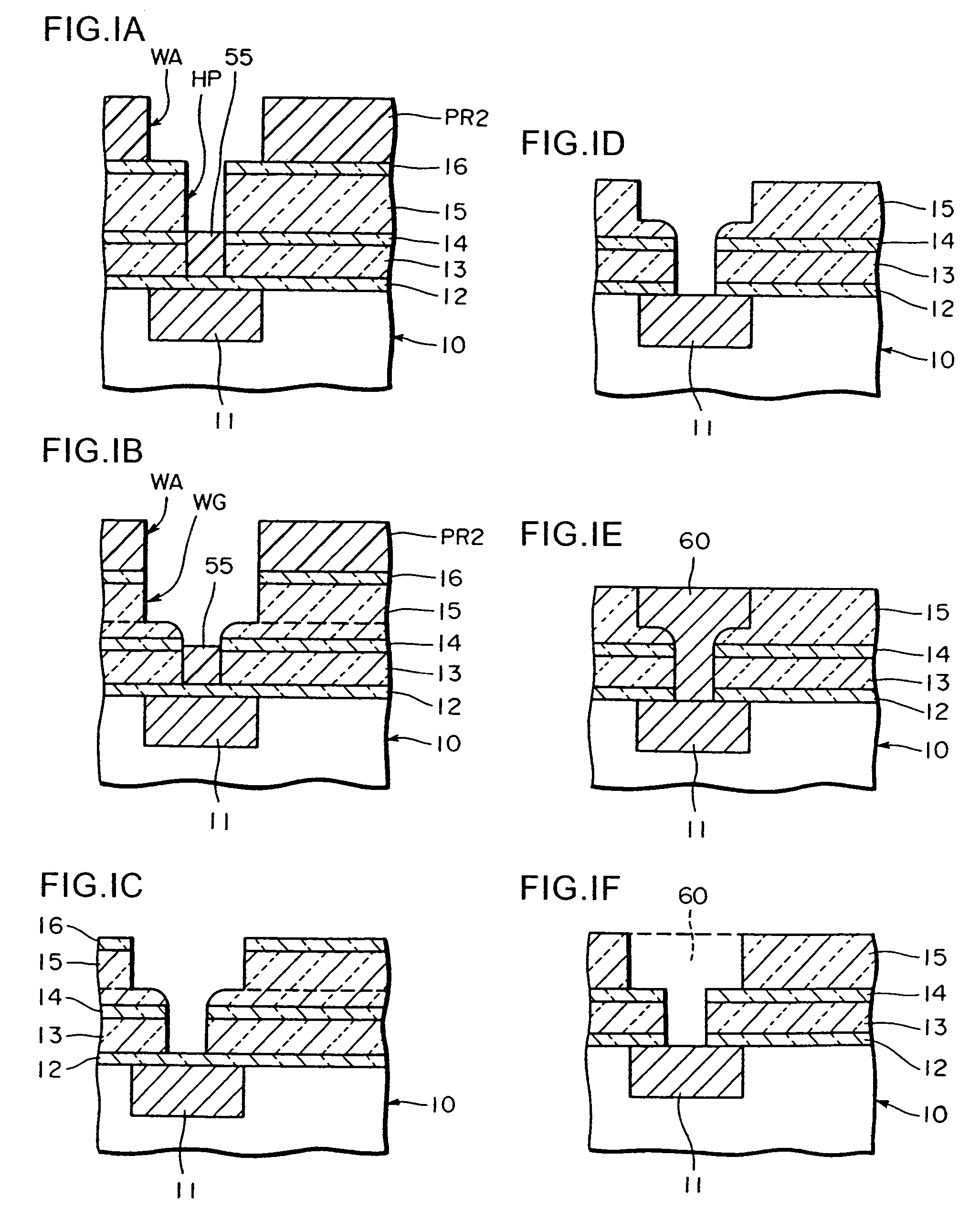
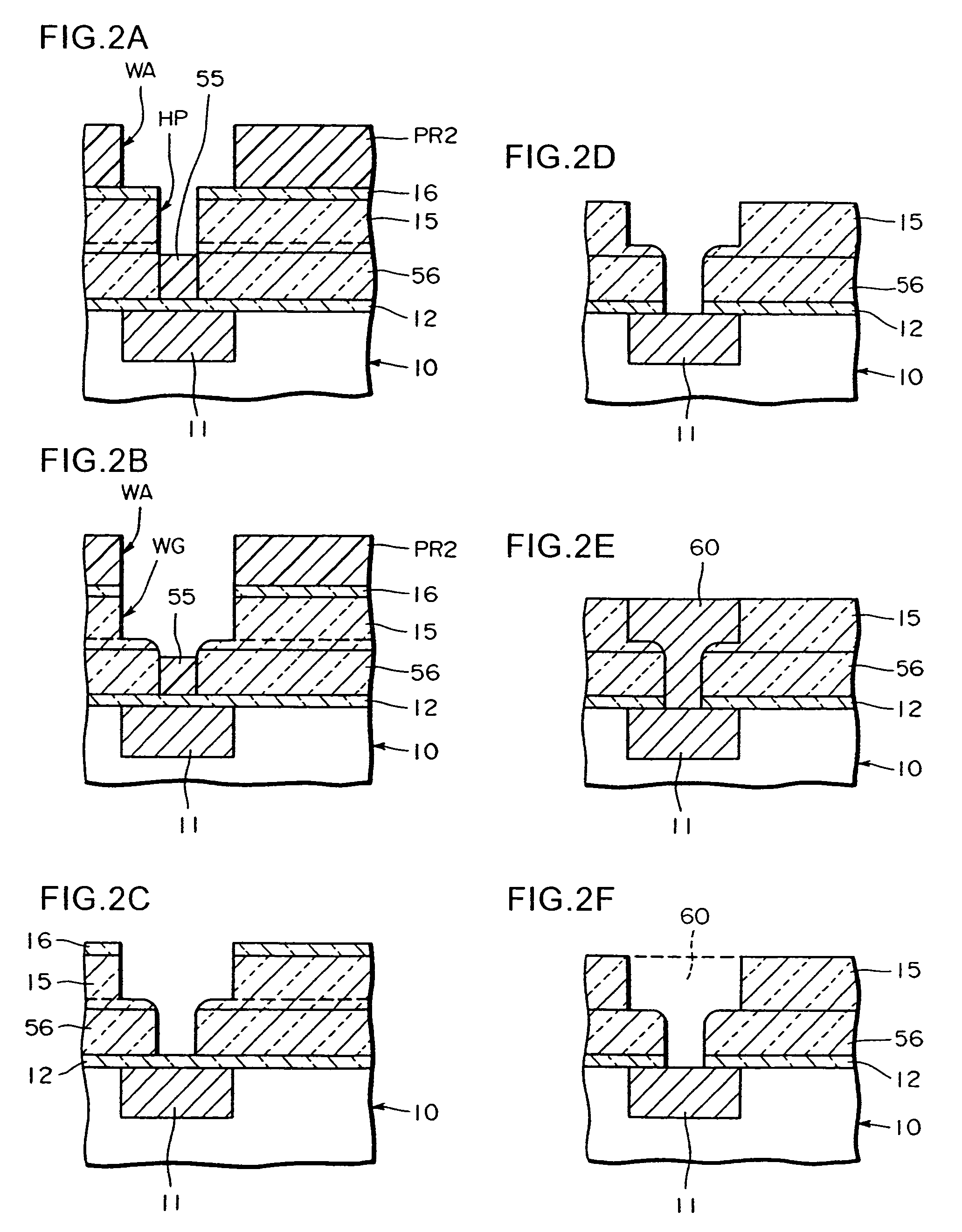
[0115]Similar to the embodiment shown in FIGS. 1A to 1E, after a resist pattern is formed on the antireflection film 16, the antireflection film 16, second and first interlayer insulating films 15 and 56 are anisotropically etched to form a via hole HP. The resist pattern is thereafter removed, and a protective filler 55 of organic compound is disposed on the bottom of the via hole HP. Similar to the first embodiment, the protective filler 55 is formed lower than the upper surface of the first interlayer insulating film 56. The first and second interlayer insulating films 56 and 15 have similar etch rates, as described above.

[0116]A resist pattern PR2 having an opening WA corresponding to a wiring trench pattern is formed on the antireflection film 16.

[0117]As shown in FIG. 2B, by using the resist pattern PR2 having the opening WA, the antireflection film 16 and second interlayer insulating film 15 are etched. The second interlayer insulating film 15 is etched through controlled etc...

second embodiment

[0130]In the second embodiment, the lower interlayer insulting film is made of plasma SiO2. A plasma SiO2 film has a low etch rate but its dielectric constant is not so low although it is lower than SiN. In order to further reduce the capacitance between upper and lower wiring layers, it is desired to use material having a much lower dielectric constant.

[0131]FIGS. 3A to 3E show the structure of an interlayer insulating film made of a plasma SiO2 film capable of suppressing abnormal etching having a limited thickness and sandwiched between fluorine containing silicon oxide films.

[0132]As shown in FIG. 3A, on an underlie 10 having a conductive region 11, a lamination structure is formed having: an etch stopper layer 12 made of SiN or the like; a first interlayer insulating film 13 made of fluorine containing silicon oxide; an etch suppressing insulating film 54 made of plasma SiO2; a second interlayer insulating film 15 made of fluorine containing silicon oxide; and an antireflection...


PUM


Abstract

A semiconductor device having: an underlie having a conductive region in the surface layer of the underlie; an insulating etch stopper film covering the surface of the underlie; an interlayer insulating film formed on the insulating etch stopper film; a wiring trench formed in the interlayer insulating film, the wiring trench having a first depth from the surface of the interlayer insulating film; a contact hole extending from the bottom surface of the wiring trench to the surface of the conductive region; and a dual damascene wiring layer embedded in the wiring trench and the contact hole, wherein the interlayer insulating film includes a first kind of an insulating layer surrounding the side wall and bottom surface of the wiring trench and a second kind of an insulating layer having etching characteristics different from the first kind of the insulating layer. The semiconductor device is provided which can protect the underlying conductive region sufficiently and has a dual damascene wiring layer having a high reliability and a small wiring capacitance.

Description

[0001]This application is a divisional application of prior application Ser. No. 09 / 735,479 filed Dec. 14, 2000, now U.S. Pat. No. 6,787,907.[0002]This application is based on Japanese Patent Application 2000-221202, filed on Jul. 21, 2000, the entire contents of which are incorporated herein by reference.BACKGROUND OF THE INVENTION[0003]a) Field of the Invention[0004]The present invention relates to a semiconductor device and its manufacture method, and more particularly to a semiconductor device having a dual damascene wiring structure and its manufacture method.[0005]In this embodiment, an “etch stopper” is intended to mean a layer having an etch rate of at most ⅕ times that of a layer to be etched. A “similar etch rate” is intended to mean an etch rate about ½ to about two times that of a layer to be etched.[0006]b) Description of the Related Art[0007]Demands for higher integration of semiconductor devices are increasing. A conventional conductive wire is made of Al, W or the li...

Claims


Application Information

Patent Timeline
Patent Type & Authority Patents(United States)
IPC IPC(8): H01L21/4763H01L21/302H01L21/461H01L23/522H01L21/3205H01L21/768
CPCH01L21/76807H01L21/76808H01L21/76813H01L21/76804H01L21/76829H01L2221/1036H01L2924/0002H01L2924/00H01L21/3205
Inventor WATANABE, KENICHIKOMADA, DAISUKESHIMPUKU, FUMIHIKO
Owner TRINITY SEMICON RES
Why Eureka
Try Eureka