Metal-oxide-semiconductor transistor and method of forming the same

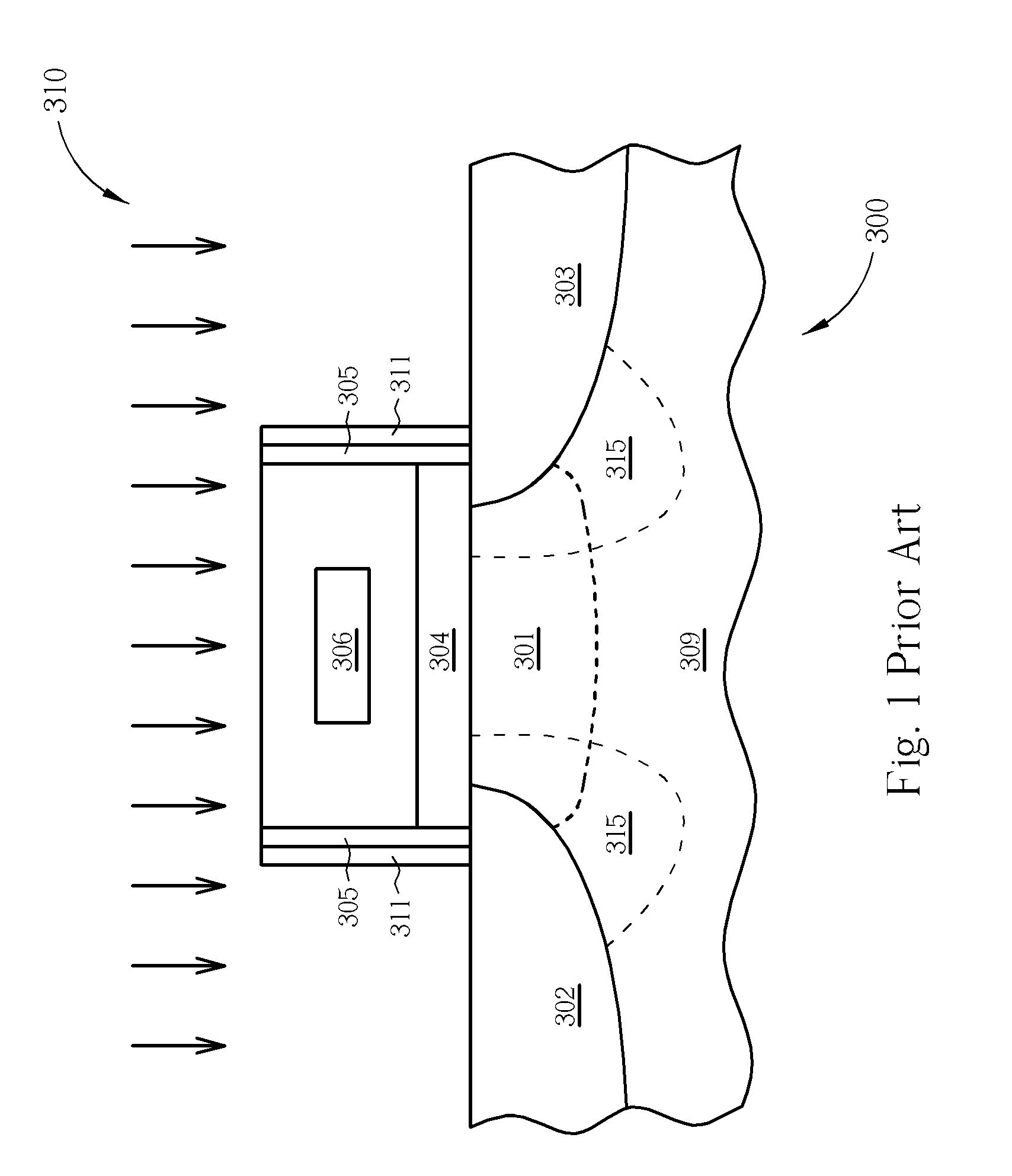
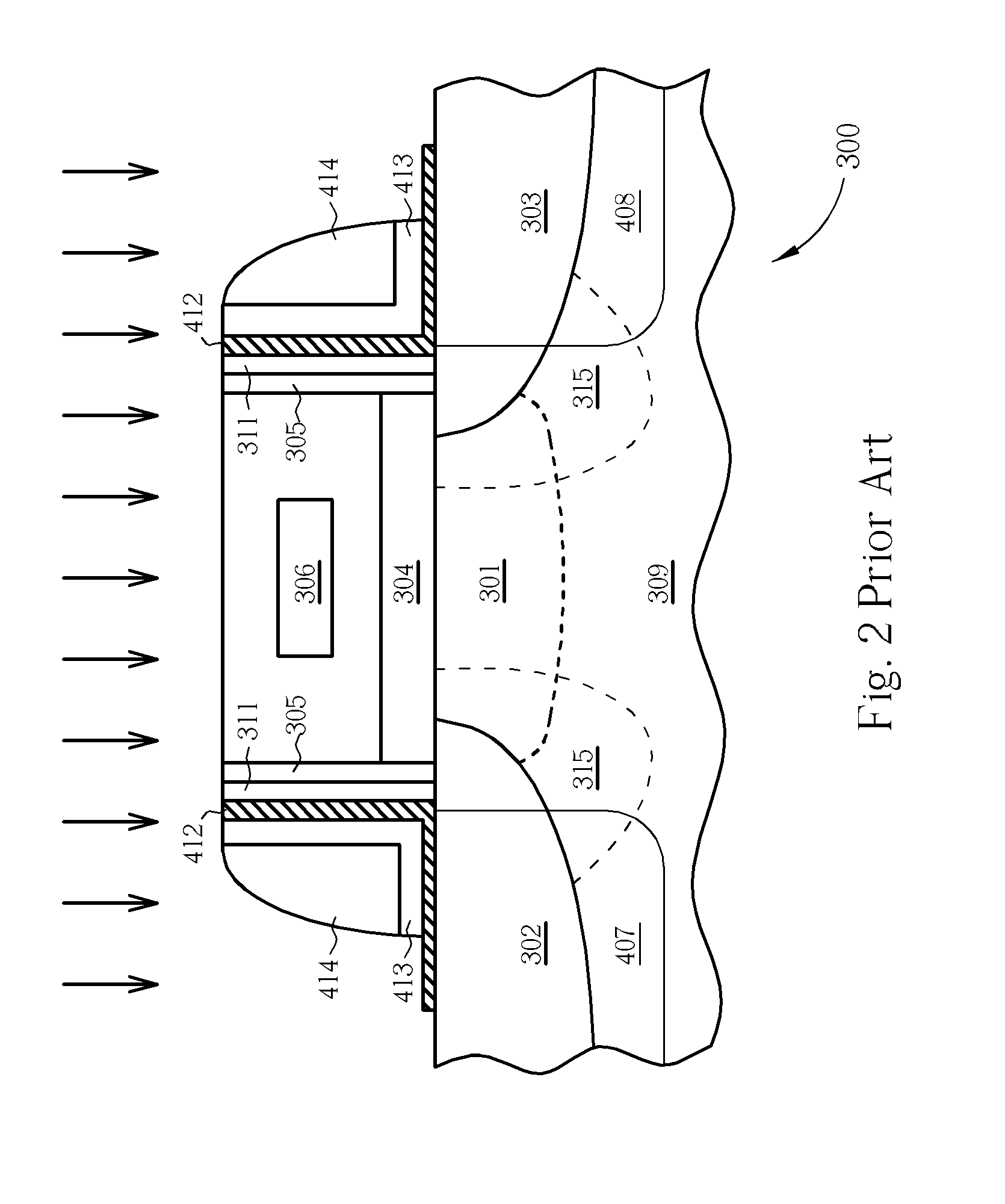
a technology of metal-oxidesemiconductor and transistor, which is applied in the direction of semiconductor/solid-state device manufacturing, semiconductor devices, electrical equipment, etc., can solve the problems of pmos composite cap b>516/b> the loss of net boron dopant in the channel, and the inability to apply pmos composite cap 516 in the prior art method, etc., to achieve the effect of developing the performance of mos

Active Publication Date: 2008-05-01
UNITED MICROELECTRONICS CORP
View PDF5 Cites 19 Cited by
  • Summary
  • Abstract
  • Description
  • Claims
  • Application Information

AI Technical Summary

Benefits of technology

[0015]Because a stressed cap layer is formed on a MOS transistor after a spacer on the MOS transistor is removed, the stressed cap layer can make a structural strain, increase a drive current of the MOS transistor, and develop the performance of the MOS transistor.

Problems solved by technology

As the semiconductor processes advance, how to increase the driving current for MOS transistors for fabrication processes under 65 nanometers has become a great challenge.
As a result, there is a net boron dopant loss in the channel, which reduces the dopant pile up at the Si / SiO2 interface.
As a result, the composite cap 516 in the prior art method cannot be applied to the PMOS, and it is still a challenge in increasing the driving current of MOS transistors.

Method used


Image

  • Metal-oxide-semiconductor transistor and method of forming the same
  • Metal-oxide-semiconductor transistor and method of forming the same
  • Metal-oxide-semiconductor transistor and method of forming the same

Examples


Embodiment Construction

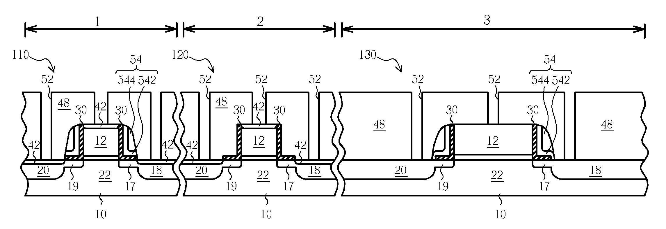
[0023]Please refer to FIGS. 7-13. FIGS. 7-13 are schematic cross-sectional diagrams illustrating a method of fabricating MOS transistors in accordance with a first preferred embodiment of the present invention, wherein like number numerals designate similar or the same parts, regions or elements. It is to be understood that the drawings are not drawn to scale and are served only for illustration purposes. It is to be understood that some lithographic and etching processes relating to the present invention method are known in the art and thus not explicitly shown in the drawings.

[0024]The present invention pertains to a method of fabricating a MOS transistor used in integrated circuits, such a N-type MOS (NMOS) transistor, a N-type MOS (PMOS) transistor or a complementary MOS (CMOS) device. For detailed description, processes for MOS transistors in different regions are demonstrated through FIGS. 7-13. As shown in FIG. 7, a semiconductor substrate 10 is prepared. The semiconductor su...


PUM


Abstract

A method of manufacturing a MOS transistor device. First, a semiconductor substrate having a gate structure is prepared. The gate structure has two sidewalls and a liner on the sidewalls. Subsequently, a stressed cap layer is formed on the semiconductor substrate, and covers the gate structure and the liner. Next, an activating process is performed. Furthermore, the stressed cap layer is etched to be a salicide block. Afterward, a salicide process is performed to form a silicide layer on the regions that are not covered by the stressed cap layer.

Description

BACKGROUND OF THE INVENTION[0001]1. Field of the Invention[0002]The present invention generally relates to the field of metal-oxide-semiconductor (MOS) transistors, and more particularly, to a method for forming MOS transistors having strained silicon. From one aspect of the present invention, a stressed cap layer is formed on a MOS transistor after a spacer on the MOS transistor is removed. As a result, the stressed cap layer can make a structural strain, increase a drive current of the MOS transistor, and develop the performance of the MOS transistor.[0003]2. Description of the Prior Art[0004]As semiconductor technology advances and development of integrated circuits revolutionizes, the computing power and storage capacity for computers also increase exponentially, which further increases the expansion of related industries. As predicted by Moore Law, the number of transistors utilized in integrated circuits has been doubled every 18 months and semiconductor processes also have ad...

Claims


Application Information

Patent Timeline
Patent Type & Authority Applications(United States)
IPC IPC(8): H01L29/76H01L29/94H01L31/00H01L21/8234H01L21/336
CPCH01L21/823807H01L21/823835H01L21/82385H01L29/7843H01L29/6653H01L29/6656H01L21/823864
Inventor LEE, KUN-HSIENHUANG, CHENG-TUNGHUNG, WEN-HANTING, SHYH-FANNJENG, LI-SHIANCHENG, TZYY-MINGCHEN, NENG-KUOHSU, SHAO-TATSAI, TENG-CHUNHUANG, CHIEN-CHUNG
Owner UNITED MICROELECTRONICS CORP
Why Eureka
Try Eureka