IGZO thin film transistor and method for improving electrical property of IGZO thin film transistor

A thin-film transistor and electrical performance technology, which is applied in the direction of transistors, circuits, electrical components, etc., can solve the problems of reducing device performance, affecting IGZO thin-film metal Schottky contacts, and many oxygen vacancy defects, so as to improve mobility and improve Oxygen vacancy defects, the effect of increasing the driving current

Inactive Publication Date: 2014-06-25
EVERDISPLAY OPTRONICS (SHANGHAI) CO LTD
View PDF2 Cites 20 Cited by
  • Summary
  • Abstract
  • Description
  • Claims
  • Application Information

AI Technical Summary

Problems solved by technology

[0007] However, in the IGZO film prepared by this patent, there may be more oxygen vacancy defects in the film, which may easily lead to the leakage current phenomenon. At the same time, the source, drain and passivation layer are directly prepared after the IGZO film is prepared. The impurities and defects existing on the surface of the IGZO film are treated, which affects the Schottky contact of the metal between the IGZO film and the source and drain, and generally reduces the performance of the device.

Method used


Image

  • IGZO thin film transistor and method for improving electrical property of IGZO thin film transistor
  • IGZO thin film transistor and method for improving electrical property of IGZO thin film transistor
  • IGZO thin film transistor and method for improving electrical property of IGZO thin film transistor

Examples


Embodiment Construction

[0032] The specific embodiment of the present invention will be further described below in conjunction with accompanying drawing:

[0033] The invention provides a method for improving the electrical performance of an IGZO thin film layer transistor. In the process of preparing a display device containing an IGZO thin film, the IGZO thin film is treated by using a plasma treatment process to improve the oxygen atom content of the IGZO thin film layer. Improve the performance of the device; at the same time, the UV radiation treatment is performed at the same time as the plasma treatment, which can further accelerate the reaction and obtain a better process effect.

[0034] Specific steps are as follows:

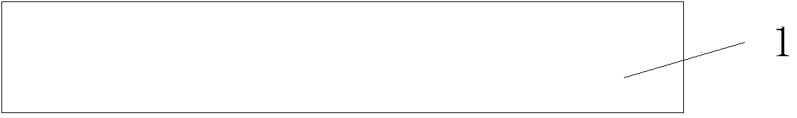
[0035] Step S1: providing a substrate 1, preferably, the substrate 1 is a glass substrate; and cleaning the substrate 1, such as figure 1 shown.

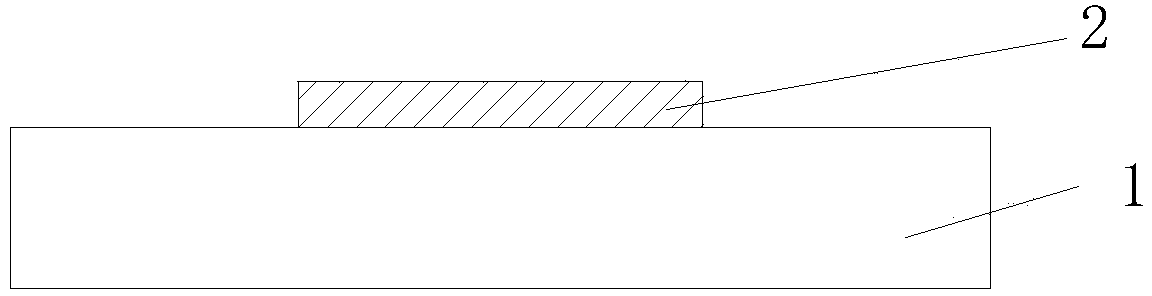
[0036] Step S2: Deposit a metal layer on the substrate 1, then perform a photolithography process and etch the metal layer, an...


PUM


Abstract

The invention provides an IGZO thin film transistor and a method for improving the electrical property of the IGZO thin film transistor. The method comprises the following steps that a semiconductor structure is provided, the semiconductor structure comprises a substrate, a metal gate is formed on part of the surface of the substrate, and the metal gate and the upper surface of the substrate are respectively covered with a gate oxide layer; an IGZO film layer is manufactured to cover the gate oxide layer, the IGZO film layer is etched to form an active layer and a pixel electrode area, and a source electrode, a drain electrode and a passivation layer are formed above the IGZO film layer in sequence; after the IGZO film layer is etched to form the active layer, the surface of the IGZO film layer is treated through a plasma treatment process. The IGZO film layer is treated through oxygen plasma and UV radiation, the oxygen content of an IGZO film is improved, lattice imperfections between the IGZO film and the gate oxide layer are reduced, meanwhile, impurities and defects on the surface of the IGZO film can be removed, and device performance is improved.

Description

technical field [0001] The invention relates to the field of display screen manufacture, in particular to an IGZO thin film transistor and a method for improving the electrical performance of the IGZO thin film transistor. Background technique [0002] IGZO (indium gallium zinc oxide) is the abbreviation of indium gallium zinc oxide. Amorphous IGZO material is a channel layer material used in the new generation of thin film transistor technology and is a kind of metal oxide (Oxied) panel technology. IGZO material was first proposed by Hideo Hosono of Tokyo Institute of Technology in Japan to be applied in the TFT industry. [0003] Using IGZO technology can make the power consumption of the display screen close to that of OLED, but the cost is lower, the thickness is only 25% higher than that of OLED, and the resolution can reach full HD (full HD, 1920*1080P) or even ultra high definition (Ultra Definition, Resolution 4k*2k) level. [0004] IGZO is currently a very popular...

Claims


Application Information

Patent Timeline
Patent Type & Authority Applications(China)
IPC IPC(8): H01L29/786H01L21/336
CPCH01L29/7869H01L21/423H01L29/66742
Inventor 鲁海生
Owner EVERDISPLAY OPTRONICS (SHANGHAI) CO LTD
Why Eureka
Try Eureka