Fin field effect transistor and forming method thereof

A fin field effect and transistor technology, which is applied in semiconductor devices, semiconductor/solid-state device manufacturing, electrical components, etc., can solve problems such as affecting transistor performance, increasing the parasitic capacitance of conductive plugs in source and drain regions, and reducing Effect of Small Parasitic Capacitance

Active Publication Date: 2014-07-16
SEMICON MFG INT (SHANGHAI) CORP
View PDF3 Cites 18 Cited by
  • Summary
  • Abstract
  • Description
  • Claims
  • Application Information

AI Technical Summary

Problems solved by technology

[0005] However, in the prior art, the sidewalls of fin field effect transistors with negative cover regions are formed with high dielectric constant materials, which increases the parasitic capacitance between the gate electrode and the subsequently formed conductive plugs in the source region and drain region, affecting Transistor performance

Method used


Image

  • Fin field effect transistor and forming method thereof
  • Fin field effect transistor and forming method thereof
  • Fin field effect transistor and forming method thereof

Examples


Embodiment Construction

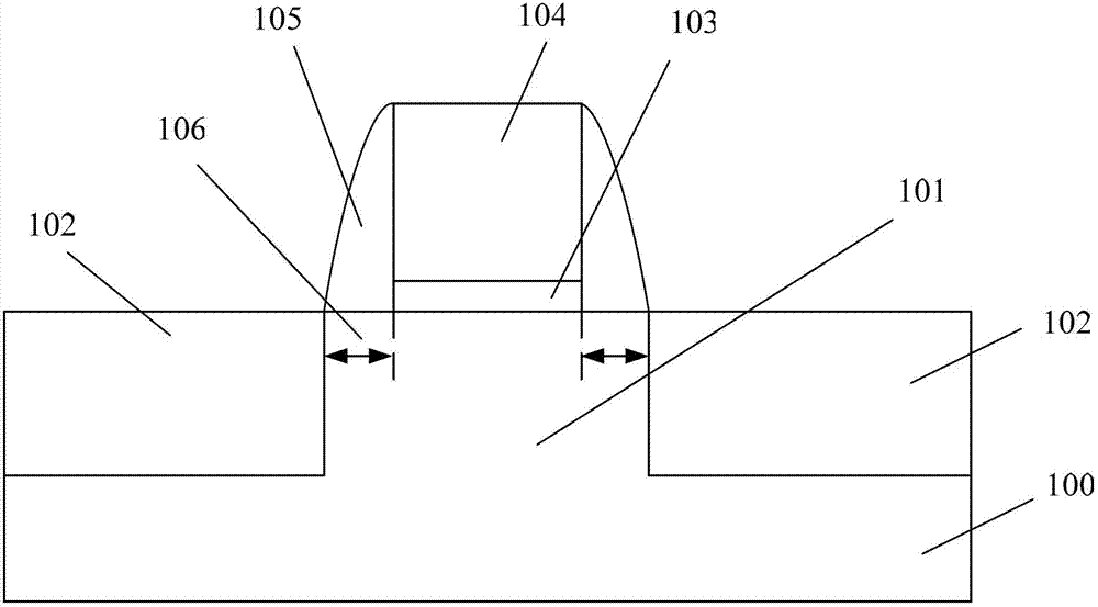
[0034] It can be seen from the background art that the parasitic capacitance between the gate electrode and the conductive plugs in the source region and the drain region of the fin field effect transistor with the negative cover region formed in the prior art is large.

[0035] The inventors of the present invention have studied the formation method of the fin field effect transistor with the negative cover region in the prior art, and found that the high dielectric constant sidewalls lead to large parasitic capacitance between the gate electrode and the conductive plugs in the source region and the drain region. the main reason. It can be seen from the formula C=εS / 4πkd that in a flat plate capacitor, the capacitance C is inversely proportional to the distance d between the plates, and is inversely proportional to the dielectric constant ε of the dielectric layer between the plates, so it can be reduced by reducing the dielectric of the sidewall material constant to reduce t...


PUM


Abstract

The invention discloses a fin field effect transistor and a forming method thereof. The forming method of the fin field effect transistor comprises: providing a semiconductor substrate, the surface of the semiconductor substrate being provided with a projection fin portion and a grid structure which is disposed on the fin portion and covers a part of the top portion and the side wall of the fin portion; forming a first dielectric layer covering the grid structure; forming a second dielectric layer covering the first dielectric layer, the dielectric constant of the second dielectric layer being smaller than the dielectric constant of the first dielectric layer; etching back the second dielectric layer, and forming a second side wall; and etching the first dielectric layer by taking the second side wall as a mask, and forming a first side wall, the first side wall being provided with a horizontal portion and a vertical portion, the part of the fin portion covered by the first side wall constituting a negative covering zone. According to the invention, the parasitic capacitance between the grid structure of the fin field effect transistor and the conductive plug of a source region and a drain region is small.

Description

technical field [0001] The invention relates to the technical field of semiconductors, in particular to a fin field effect transistor and a forming method thereof. Background technique [0002] MOS transistors generate switching signals by regulating the current through the channel region by applying a voltage to the gate. With the development of semiconductor technology, the control ability of the traditional planar MOS transistor on the channel current becomes weaker, resulting in serious leakage current. Fin Field Effect Transistor (Fin FET) is an emerging multi-gate device, which generally includes a semiconductor fin protruding from the surface of the semiconductor substrate, and a gate structure covering part of the top and side walls of the fin, A source region and a drain region are located in the fins on both sides of the gate structure. [0003] But below the 20nm node, the thickness of the fin field effect transistor fin is extremely small, and the short channel...

Claims


Application Information

Patent Timeline
Patent Type & Authority Applications(China)
IPC IPC(8): H01L21/336H01L29/78
CPCH01L29/42364H01L29/66795H01L29/785
Inventor 三重野文健殷华湘
Owner SEMICON MFG INT (SHANGHAI) CORP
Why Eureka
Try Eureka